5G communication PCB
HDI PCB: Standards, Cost Breakdown & Manufacturing Guide
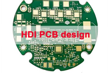
The standard minimum trace width and spacing for industrial HDI PCB per official IPC 2226 standard is 25μm for inner layers and 30μm for outer layers for stable mass production, while ultra-fine prototype HDI designs adopt 20μm trace spacing matched with professional laser microvia fabrication for consumer electronics and automotive Read more