
The standard minimum trace width and spacing for industrial HDI PCB per official IPC 2226 standard is 25μm for inner layers and 30μm for outer layers for stable mass production, while ultra-fine prototype HDI designs adopt 20μm trace spacing matched with professional laser microvia fabrication for consumer electronics and automotive electronic projects.
High Density Interconnect (HDI) PCBs are advanced circuit substrates embedded with microvias, ultra-fine conductive traces and high-density pad layouts manufactured per IPC 2226 global industrial standards. Different from conventional rigid FR-4 PCBs, HDI PCBs adopt blind vias, buried vias and any-layer microvia structures to optimize inner routing layout, which serves as core circuit carriers for 5G communication modules, automotive electronics and medical electronic devices across global North American industrial supply chains.
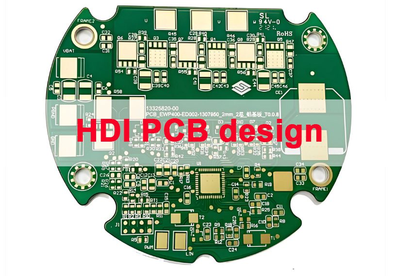
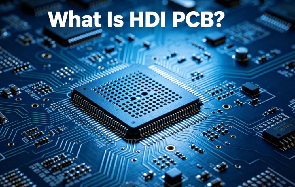
What Is HDI PCB
HDI PCB, short for High Density Interconnect Printed Circuit Board, is a high-precision printed circuit board with ultra-fine traces, miniature micro-holes and compact pad density beyond conventional standard PCB manufacturing limits. Defined by IPC-2226 international unified industrial standard, HDI PCBs feature microvias smaller than 150μm, reduced pad pitch and stacked via structures to maximize wiring density within limited board dimension. It abandons traditional mechanical through-via manufacturing process, applying laser ablation and multi-time lamination processes to realize high-density inner circuit interconnection for miniaturized high-performance electronic terminals.
Industry verified data shows HDI PCB wiring density is 2 to 3 times higher than ordinary standard rigid PCBs, solving high-density wiring bottlenecks for compact multi-functional industrial electronic modules.
HDI PCB Vs Standard PCB
Core differences between HDI PCB and standard PCB focus on via structure, trace precision, manufacturing workflow, raw material selection and applicable industrial scenarios, with clear gaps in production difficulty, mass production yield and overall procurement budget. Standard PCBs only adopt mechanical through-vias and general rolled copper foil, while HDI PCBs apply laser-drilled microvias, professional RCC materials and multi-cycle stacked lamination processes for higher circuit integration performance.
| Comparison Parameter | HDI PCB | Standard FR-4 PCB | US Project Applicability |
| Minimum Trace Spacing | 25μm-50μm | 100μm-150μm | High-end consumer, automotive electronics |
| Via Drilling Method | Laser Drilling, Blind/Buried Microvias | Mechanical Drilling, Through-vias Only | Low-cost industrial control equipment |
| Average Unit Cost | Noticeably Higher | Basic Industrial Bulk Price | Cost-sensitive mass orders |
| Mass Production Lead Time | 7-18 Working Days | 3-7 Working Days | Urgent US OEM prototype orders |
| IPC Compliance Grade | IPC 2226 Class 2/3 | IPC 6012 Basic Grade | Aerospace, medical certified projects |
Standard PCBs fit low-density industrial control hardware, while HDI PCBs are mandatory components for 5G modules, wearable devices and new energy vehicle core boards to meet standard electromagnetic compatibility requirements.
Benefits Of High Density Interconnect PCB
High density interconnect PCBs own core industrial advantages verified by global PCB manufacturing engineering practices, matching North American electronic design optimization and cross-border supply chain demands. Firstly, ultra-high wiring density shrinks overall PCB footprint to support portable, miniaturized electronic product design. Secondly, shortened conductive traces reduce high-frequency signal attenuation and electromagnetic crosstalk for RF and 5G circuit modules.
Thirdly, stacked microvia structures save inner substrate routing space to improve circuit bearing capacity. Fourthly, optimized thermal layout accelerates component heat dissipation and extends electronic product service lifespan. Fifthly, standardized modular layout simplifies SMT surface mounting procedures to lower assembly labor inputs. Sixthly, IPC 2226 compliant substrate structure improves mechanical shock resistance and corrosion resistance for outdoor industrial working environments.
For B2B electronic buyers, qualified HDI PCB assemblies lower overall product failure risks compared with standard PCBs, cutting long-term after-sales maintenance and product replacement costs for electronic brand manufacturers.
Types Of Microvias In HDI PCB
HDI PCB microvias are divided into four mainstream industrial categories based on lamination sequence and vertical penetration depth with unified industry classification standards. Core classifications include stacked microvias, staggered microvias, skip microvias and any-layer free microvias, with fixed manufacturing workflows and matched layer stackup schemes for each type.
Stacked microvias are widely adopted for conventional 1+N+1 HDI structures; staggered microvias reduce lamination pressure risks for high-layer HDI substrates; skip microvias optimize high-frequency impedance stabilization; any-layer microvias belong to advanced HDI layout for high-end medical and aerospace circuit boards. All industrial microvia designs adopt laser drilling instead of mechanical drilling to meet standard electronic safety requirements for hole wall smoothness.
Difference Between Blind And Buried Vias In HDI
Blind vias and buried vias are two mainstream non-through microvia types for HDI PCB fabrication, differing in penetration position, manufacturing sequence, process difficulty and applicable layer stackup solutions. Blind vias connect outer PCB layers with adjacent inner layers and expose on board outer surface; buried vias link two inner substrate layers and are fully enclosed inside finished PCBs without outer openings.
Buried vias require pre-lamination drilling and electroplating procedures, bringing extra process steps and higher production costs; blind vias are processed after outer layer lamination with lower technical difficulty. For mainstream North American consumer electronic HDI projects, blind vias are the preferred option; high-layer automotive HDI boards adopt combined via layouts to balance manufacturing cost and structural performance.
HDI PCB Laser Drilling Vs Mechanical Drilling
Laser drilling acts as standard manufacturing process for HDI PCB microvias, while mechanical drilling is only applicable for large-diameter holes on standard PCBs, with clear gaps in machining precision, minimum hole size, material compatibility and mass production stability. Mechanical drilling cannot process microvias under 150μm, and easily damages thin RCC base materials, which is incompatible with fine-pitch HDI design standards.
UV laser drilling supports ultra-small microvia machining below 50μm, delivers burr-free smooth hole walls, adapts thin RCC prepreg and HDI core substrates, and improves overall mass production stability of fine-pitch HDI boards. Although laser drilling increases single-board processing expenditure, it reduces post-production defect rejection and rework workload for bulk cross-border HDI orders.
HDI PCB Design Guidelines
Universal HDI PCB design guidelines comply with official IPC 2226 industrial standards and global senior PCB engineering summaries, covering microvia arrangement, trace routing, pad layout and raw material matching core constraints for cross-border mass production. Designers need to arrange microvias in staggered distribution to avoid substrate delamination, limit dense stacked via concentration, and reserve standard safety clearance for impedance-controlled traces.
Targeted design rules for electronic projects: Reserve shielding space for high-frequency circuits to meet EMI requirements, adopt RoHS 2.0 halogen-free compliant substrates, and unify design parameters to pass commodity compliance audits. Standardized HDI design rules lower DFM revision frequency for electronic design teams.
HDI PCB Layer Stackup Examples
Global mainstream industrial HDI PCB layer stackup schemes cover four classic commercial structures matching international electronic project demands: 2-layer 1+0+1 basic HDI stackup, 6-layer 1+4+1 medium-density stackup, 10-layer 2+6+2 high-layer stackup and 8-layer any-layer HDI stackup. Each stackup matches fixed copper foil specification, prepreg thickness and microvia stacking rules.
1+0+1 basic stackup features dual outer microvia layers without inner buried vias for low-cost wearable device HDI boards; 2+6+2 stackup applies double-sided stacked microvias for automotive sensor circuit substrates; any-layer stackup supports arbitrary interlayer connection for precision medical equipment HDI PCBs. All listed stackup schemes are verified by standardized mass lamination production workflows.
Minimum Trace Width And Spacing For HDI PCB
Per IPC 2226 official classification standard, Class 3 high-reliability HDI PCBs for aerospace and medical industrial projects adopt 20μm minimum trace width and 25μm minimum trace spacing; Class 2 commercial industrial HDI PCBs for consumer electronics use 30μm trace width and 35μm trace spacing for stable mass production.
For ultra-thin 0.4mm HDI core substrates, mainstream PCB manufacturers expand basic trace spacing properly to prevent copper trace open-circuit risks during high-pressure lamination, solving common structural design defects summarized by global HDI PCB engineering communities.
1+N+1 Vs 2+N+2 HDI PCB Structure
1+N+1 and 2+N+2 are two dominant stacked HDI PCB industrial structures differentiated by outer microvia lamination cycles and inner core layer quantities. The letter N stands for inner standard core PCB layer number; numeric digits represent outer stacked microvia lamination layers, determining overall board precision, manufacturing budget and high-density wiring capacity.
| Structure Item | 1+N+1 HDI Structure | 2+N+2 HDI Structure |
| Outer Lamination Times | 1 Time Double-sided Lamination | 2 Times Double-sided Lamination |
| Max Microvia Density | Medium Density | Ultra-high Density Stacked Vias |
| Relative Fabrication Cost | Base HDI Cost | Higher Unit Production Cost |
| Typical US Application | Smart home, 4G module PCB | 5G RF, automotive ECU PCB |
| Average Lead Time | 7-10 Working Days | 12-16 Working Days |
Anylayer HDI PCB Design Rules
Anylayer HDI PCB design rules break fixed layer stacking limits of conventional 1+N+1 and 2+N+2 HDI structures, supporting arbitrary interlayer microvia connection without fixed inner routing restrictions, fully compliant with IPC 2226 Class 3 high-reliability design specifications. This standard cancels mandatory buried via layout limits and releases inner layer routing space to maximize wiring utilization rate.
Universal industrial mandatory constraints: Avoid stacked via vertical overlapping, follow 50μm minimum pad clearance standard, match dedicated thin RCC copper foil substrates, and control finished board warpage within industrial qualified threshold for precision electronic assembly. Anylayer design improves layout flexibility significantly yet increases overall manufacturing difficulty and raw material procurement budget.
HDI PCB Via In Pad Design Guidelines
Via-in-pad layout is a core standardized design rule for fine-pitch BGA chip packaging on HDI PCBs, with unified specifications for international electronic designers and professional PCB manufacturers. Core industrial requirements adopt resin-filled microvias inside SMT component pads to eliminate hollow pad defects, prevent solder overflow and optimize SMT mounting yield.
Global PCB engineering practical guidelines: Apply copper-plated resin filled vias for ultra-fine BGA pad layouts; ban unfilled laser microvias on surface mounting pads; control microvia offset within industrial tolerance range; select low-stress prepreg substrates to reduce pad delamination risks during reflow soldering procedures. This specification solves common SMT assembly defects of high-precision HDI circuit boards.
How To Control Impedance In HDI PCB Layout
HDI PCB impedance stabilization relies on calibrated dielectric substrate thickness, standard copper foil thickness and precise trace width adjustment, matched with fixed dielectric constant of professional RCC materials to stabilize 50Ω and 90Ω high-frequency impedance for RF and 5G North American circuit projects. Different from standard PCBs, HDI fine traces require real-time process parameter calibration to avoid impedance deviation risks.
Standard manufacturer impedance control workflow: Confirm IPC certified dielectric substrate parameters before mass production; partition impedance traces and microvia zones; reduce parasitic capacitance of stacked microvias; reserve standard impedance test coupons on board edges; finish offline electrical testing before bulk shipment. Standardized layout control minimizes impedance mismatch defects for cross-border bulk HDI orders.
IPC 2226 HDI PCB Design Standards
IPC 2226 is the exclusive global unified industrial standard dedicated to HDI and microvia printed circuit boards, certified and recognized by US UL, FCC and North American electronic manufacturing associations. It covers raw material screening, microvia dimension tolerance, layer alignment, mechanical tolerance, reliability testing and product classification systems for HDI production.
This standard divides finished HDI PCBs into three reliability grades: Class 1 for consumer electronics, Class 2 for general industrial equipment, Class 3 for aerospace and medical high-reliability devices. Core US market compliant parameters include unified layer alignment tolerance, cyclic thermal shock resistance and electronic substrate environmental requirements, matching North American commodity customs and quality audit standards.
Why Is HDI PCB Manufacturing Cost So High
Elevated HDI PCB manufacturing costs stem from premium specialized raw materials, high-precision production equipment investment, multi-cycle lamination workflows, strict quality inspection procedures and controlled mass production yield, fitting core cost inquiry pain points of global cross-border B2B PCB buyers. Firstly, customized RCC resin-coated copper foil costs more than ordinary FR-4 copper foil for standard PCBs.
Secondly, professional UV laser drilling equipment and automatic layer alignment production lines require high fixed asset investment. Thirdly, repeated lamination and electroplating workflows extend production cycles and increase labor and energy consumption. Fourthly, ultra-fine trace and microvia processes bring stricter production control, raising qualified product control costs. Fifthly, international third-party certification and export compliance testing generate extra operational overheads.
How To Reduce HDI PCB Fabrication Cost
Summarized from global professional HDI PCB manufacturing engineering experiences, feasible optimization solutions cut overall fabrication costs without downgrading IPC 2226 certified product quality, suitable for North American bulk electronic procurement budget control. Adopt conventional 1+N+1 stacked structure to replace high-cost 2+N+2 and any-layer layouts for general commercial projects; select qualified domestic certified raw materials to replace overpriced imported substrates reasonably.
Optimize microvia layout quantity to lower laser machining workload; unify repeated layer stackup schemes to shorten production line setup time; cancel redundant high-grade reliability tests for commercial-grade orders; combine scattered bulk orders to reduce unit production and cross-border logistics costs. These industry-verified optimizations lower overall procurement expenditure for international electronic bulk purchasers.
RCC Vs Standard Copper Foil For HDI Cost Comparison
RCC (Resin Coated Copper) foil and conventional rolled standard copper foil are two mainstream conductive base materials for HDI PCB production, with clear gaps in raw material budget, laser process compatibility and mass production defect rate, directly influencing total HDI board manufacturing expenditure. RCC foil is customized for high-grade laser microvia HDI fabrication; standard copper foil only adapts basic low-density 1+N+1 HDI structures.
| Comparison Item | RCC Copper Foil | Standard Copper Foil | HDI Cost Impact |
| Unit Raw Material Price | Higher Material Cost | Basic Raw Material Cost | Raise total board manufacturing budget |
| Laser Drilling Adaptability | Perfect for Fine Microvias | Prone To Hole Burr Defects | Increases post-process rejection cost |
| Applicable HDI Type | 2+N+2, Any-layer HDI | 1+N+1 Basic HDI | Material selection decides structural cost |
Top HDI PCB Manufacturers In China
Certified top Chinese HDI PCB manufacturers serving North American cross-border supply chains own complete IPC 2226 process certification, high-layer any-layer HDI production capacity and US UL, RoHS export compliance qualifications, covering prototype sample development and large-scale batch mass production services. Leading domestic manufacturers focus on automotive, medical and 5G high-layer HDI standardized production for global overseas clients.
We are a professional China-origin HDI PCB direct source manufacturer with standardized independent laser drilling workshops and Class 3 IPC compliant production lines, supplying global clients without intermediate agents. We support overseas client custom prototype development, OEM and ODM bulk manufacturing, and matched PCBA one-stop services, providing complete factory audit documents for international enterprise supplier qualification reviews.
HDI PCB Manufacturing Capabilities Checklist
This universal HDI PCB manufacturing capability audit checklist is customized for procurement engineers and quality audit teams, covering core audit modules including production equipment, process range, industry standards, raw material control, delivery cycle and export certification, widely adopted in the electronic manufacturing industry.
- Laser drilling equipment: Professional UV laser machines for standard microvia precision machining
- Layer capacity: Support 2-24 layer 1+N+1, 2+N+2, any-layer HDI volume fabrication
- Industry certification: IPC2226, UL, RoHS 2.0, US FCC cross-border export compliance certificates
- Raw material audit: Qualified industrial RCC copper foil, halogen-free prepreg raw material supply chain
- Quality control: Professional impedance testing, microvia tomography, thermal shock reliability testing
- US supply service: Standard cross-border logistics, English engineering support, batch quality inspection reports
High Layer Count HDI PCB Lead Time
Standard production lead time of high layer count HDI PCB (10 layers and above) for US clients is divided into prototype sample cycle and bulk mass production cycle per mainstream Chinese factory production schedules. 10-16 layer 2+N+2 HDI prototype production takes 10-12 working days; standardized bulk batch production takes 16-18 working days.
18-24 layer any-layer ultra-high density HDI PCBs require 14 working days for sample fabrication and 20-22 working days for bulk shipment. Qualified manufacturers support priority production for urgent overseas high-layer HDI orders; matched sea freight and air freight cross-border logistics serve North American client delivery demands steadily.
Anylayer HDI PCB Fabrication Price Estimate
China source factory ex-works anylayer HDI PCB quotation standards for North American markets are determined by core factors including layer quantity, board dimension, copper thickness and order batch size, with transparent pricing and hidden cross-border service fees excluded. Prototype small-batch anylayer HDI orders adopt independent unit pricing standards for engineering sample development.
Large-volume bulk anylayer HDI orders enjoy factory batch discount to cut unit procurement cost; extra payable items include official export certification testing, customized impedance inspection and cross-border customs service fees. Compared with local North American HDI suppliers, qualified Chinese direct manufacturers deliver obvious total cost advantages for industrial bulk HDI procurement projects.
HDI PCB Frequently Asked Questions
Q1: Can HDI PCB replace standard PCB for US industrial control equipment? A: It is technically feasible but economically unreasonable. Ordinary industrial control circuit boards do not require microvia high-density wiring structures, so standard PCBs control overall procurement budget better. Only compact high-frequency industrial modules adopt HDI boards to balance performance and procurement cost.
Q2: Are China-made HDI PCBs compliant with US California RoHS regulations? A: Qualified China source factory HDI products adopt halogen-free substrates and lead-free electroplating processes, pass third-party RoHS 2.0 and California Prop 65 environmental testing, providing official test reports for US customs clearance and enterprise supplier quality audits directly.
Q3: What is the main failure mode of mass-produced HDI PCB for US automotive projects? A: Per global HDI PCB industry public failure analysis archives, microvia delamination and high-frequency impedance drift are two common mass production defects, mainly caused by unqualified lamination parameters and substandard raw material substrates during manufacturing.
Q4: Does via in pad design increase HDI PCB manufacturing cost obviously? A: Resin-filled via in pad layout adds extra resin filling and surface polishing procedures, raising basic manufacturing expenditure moderately, yet optimizing BGA SMT mounting stability and reducing assembly rejection losses for electronic manufacturers.
Q5: Is mechanical drilling available for low-budget HDI PCB small orders? A: No. Mechanical drilling cannot meet IPC 2226 HDI microvia dimension standards, easily causes hole wall cracks and internal circuit short circuits, and fails official HDI quality inspection; all formal HDI production requires professional laser drilling workflow.
Q6: How to shorten high layer count HDI PCB lead time for urgent US orders? A: Adopt mature fixed layer stackup schemes, cancel non-custom mandatory extra testing, confirm Gerber design files one-time without revision, and apply manufacturer priority production assembly lines to compress production cycle stably.
Q7: What raw material is the most cost-saving for commercial-grade HDI PCBs? A: Certified domestic industrial RCC copper foil matched with conventional 1+N+1 stackup is the optimal cost-performance solution, meeting international commercial quality standards while avoiding premium imported raw materials and high-cost any-layer structures.
Q8: What IPC class is required for US medical device HDI PCB? A: US FDA-supervised medical electronic HDI PCBs require IPC 2226 Class 3 high-reliability certification, with stricter thermal shock, fatigue resistance and structural stability testing than general Class 2 commercial HDI circuit boards.
Q9: Why anylayer HDI PCB has higher rejection rate than stacked HDI? A: Anylayer HDI requires multi-angle laser drilling and repeated high-pressure lamination workflows, bringing higher risks of layer offset and microvia misalignment; professional manufacturers adopt high-precision alignment equipment to stabilize mass production qualified rate.
Q10: Can we get free DFM design check for US HDI PCB Gerber files? A: As professional Chinese direct HDI PCB manufacturer, we provide complimentary English DFM layout audit, design optimization and impedance simulation for all overseas client Gerber files to fix potential design defects before formal production.
Q11: What cross-border tariff advantages do China HDI PCBs have for US buyers? A: Standard industrial PCB commodities follow official US cross-border electronic material tariff policies; our team provides complete standardized customs declaration documents to simplify customs clearance and reduce customs detention risks for North American procurement teams.
Q12: Is HDI PCB surface finish compatible with US automatic SMT production lines? A: Yes. Lead-free HASL, ENIG and ENEPIG mainstream HDI surface finishes match universal North American automatic SMT soldering temperature and assembly parameters without extra production line adjustment.
Q13: How to verify HDI PCB manufacturer’s real manufacturing capacity before bulk order? A: Follow the standardized manufacturing capability checklist to audit production workshops, professional equipment, complete industry certifications and past overseas bulk delivery cases, and avoid intermediate trading suppliers without independent production workshops.
Q14: Does high trace density of HDI PCB reduce board thermal dissipation performance? A: Professional HDI layout adds reserved thermal relief pads and copper pouring zones for heat dissipation; standardized IPC 2226 design balances high wiring density and thermal conductivity for long-term industrial electronic equipment operation.
Q15: What after-sales support is provided for US bulk HDI PCB orders? A: We provide professional English engineering technical support, batch product re-inspection, process defect analysis and free replacement for unqualified products, plus long-term fixed-cycle delivery solutions for overseas brand electronic enterprises.
Final Summary & Professional Procurement Suggestion
Core technical conclusion: Mainstream HDI PCB product lines including 1+N+1, 2+N+2 and any-layer structures comply with unified IPC 2226 international industrial standards. Laser microvia machining and specialized RCC copper foil are core process and material foundations, while blind/buried via layout and precise impedance control determine finished board performance for automotive, medical and 5G electronic projects. Elevated manufacturing costs derive from multi-step lamination and premium specialized materials, and scientific structure and material selection effectively cut procurement costs without quality degradation.
Professional selection suggestion: Cost-controlled North American commercial projects adopt 1+N+1 HDI with standard copper foil; high-reliability automotive and RF circuit modules select 2+N+2 RCC-based HDI; high-end medical and aerospace devices deploy IPC Class 3 any-layer HDI PCBs. Avoid over-specification design to eliminate redundant budget waste, and match design schemes with US local electronic industry compliance requirements.
B2B procurement suggestion: US industrial electronic buyers prioritize qualified Chinese original HDI PCB manufacturers with complete UL and IPC export certifications. Audit factory production capacity via the official checklist, confirm production lead time and cross-border logistics plans in advance, and cooperate with direct source factories to remove middle agent markup and stabilize cross-border supply chain quality.
If you’re sourcing reliable PCB/PCBA manufacturing — OEM, ODM, prototyping, mass production, or custom engineering solutions — reach out to our engineering team for technical support and a quote at sales@pcbtry.com.


0 Comments