

What Is 5G Communication PCB?
A 5G communication PCB refers to a printed circuit board designed specifically for high-frequency, high-speed data transmission required by 5G networks. Unlike traditional PCBs, a 5G PCB must handle signals in the millimeter-wave frequency range, which ranges from 24 GHz to 100 GHz, depending on the application. These PCBs are used in devices such as smartphones, routers, small cells, and 5G base stations, all of which require reliable, low-loss signal transmission.
In a 5G system, the PCB isn't just a structural platform for components—it’s also a critical conduit for high-frequency signals. This means every material choice, layer count, and trace routing detail must support minimal signal loss and strong electromagnetic shielding.
Types of 5G PCBs
Different types of 5G PCBs are used in various parts of the 5G ecosystem. Here's a quick overview:
- 5G RF PCB: Handles radio frequency signals for antennas and RF modules.
- High-speed digital PCBs: Found in 5G routers and smartphones, optimized for rapid signal switching and processing.
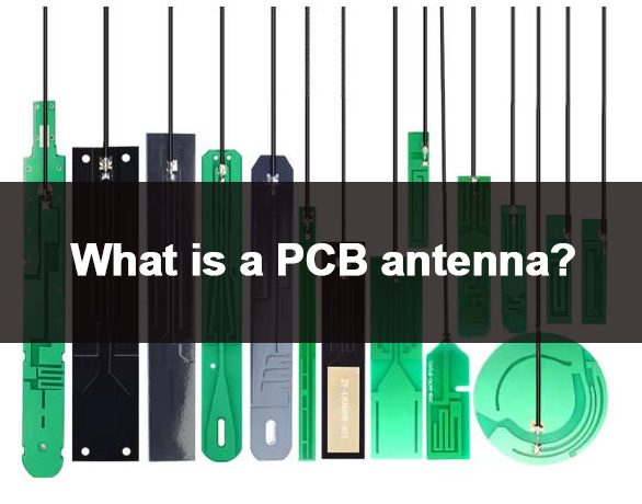
- 5G antenna PCB: Used in beamforming antenna arrays for better signal coverage.
- Base station PCBs: Multi-layer boards with power distribution, signal transmission, and heat management capabilities.
Each type varies in layer count, material composition, and design complexity, depending on whether it's used in consumer devices or industrial infrastructure.
Why Is 5G Important for PCBs?
With the shift to 5G networks, data rates, latency, and device density requirements have all increased. This directly impacts PCB design and functionality in three ways:
- Higher Frequencies: 5G operates at much higher frequencies than 4G, demanding materials with low dielectric loss to avoid signal degradation.
- Miniaturization: Devices are getting smaller, so PCBs must pack more functionality into compact, multi-layer structures.
- Thermal Management: Higher data rates and power levels generate more heat. Efficient heat dissipation becomes crucial to prevent signal distortion.
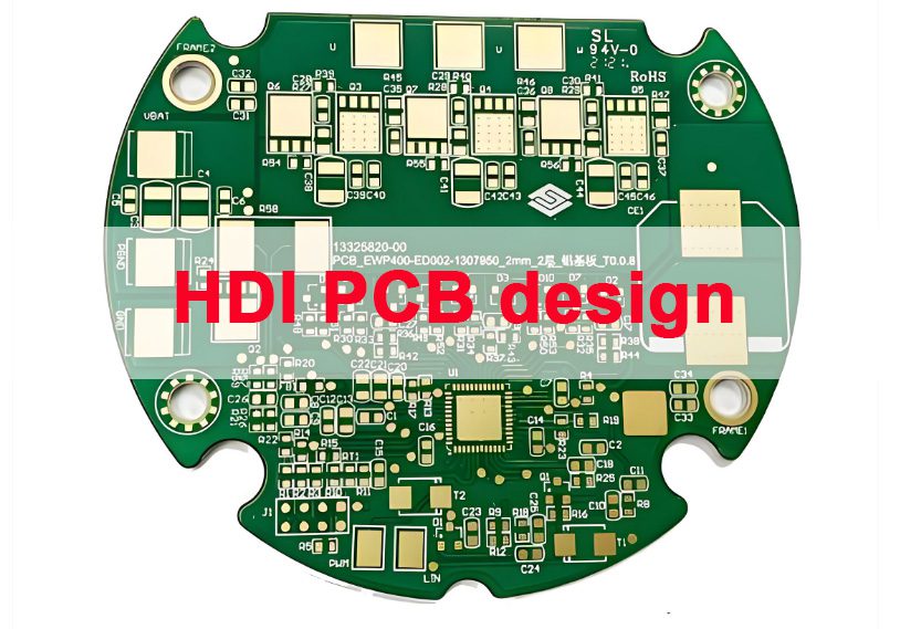
5G PCB Design Requirements
Designing a 5G PCB requires careful planning because these boards handle high-frequency signals that are more sensitive to loss, interference, and temperature changes than traditional PCBs. To ensure optimal performance, several key requirements must be met during the design phase.
1. Material Selection for High-Frequency Signals
One of the most critical decisions in 5G PCB design is choosing the right substrate material. Traditional FR4 material is not suitable for 5G because it has high dielectric loss, especially above 10 GHz. Instead, designers need low-loss, high-frequency laminates such as:
- Rogers 4350B / 4003C
- Taconic RF-35 / TLY
- Isola I-Tera / Astra
- PTFE-based materials (Teflon)
These materials have low dielectric constant (Dk) and low dissipation factor (Df), which helps maintain signal integrity and reduces signal loss at higher frequencies.
2. Controlled Impedance Management
Impedance values are typically 50Ω for single-ended traces and 90Ω to 100Ω for differential pairs. Designers must consider trace width, trace spacing, and dielectric thickness to calculate and maintain correct impedance.
3. Multilayer Stackup Design
Most 5G PCBs are multilayer, often with 6 to 12 layers or more, depending on complexity. The layer stack-up must be designed to:
- Separate signal and ground planes to reduce noise.
- Support controlled impedance routing for high-speed signals.
- Allow for power distribution layers with minimal voltage drop.
A well-planned stackup also aids in electromagnetic shielding and thermal management.
4. Via Design Considerations
Vias in 5G PCBs can introduce signal reflections and losses if not carefully designed. Some advanced via techniques include:
- Blind and Buried Vias: Used to connect inner layers without affecting surface routing.
- Back Drilling: Removes unused via stubs that can cause signal reflection.
- Via-in-Pad: Saves space and helps with thermal and signal performance, but requires filled and plated vias to avoid solder issues.
5. EMI/EMC Control
At 5G frequencies, electromagnetic interference (EMI) becomes a bigger issue. To prevent interference and ensure electromagnetic compatibility (EMC):
- Use ground planes to isolate signal layers.
- Place ground vias around high-speed signal traces.
- Design with shielded enclosures or EMI absorbing materials when needed.
Following EMI/EMC design rules helps maintain signal clarity and reduces radiated noise.
5G PCB Layout Design Considerations
Proper layout design is crucial in 5G circuit boards, especially when handling signals in the millimeter-wave range. Key considerations include:
- Signal Isolation: Prevent interference between analog and digital sections using ground planes and shielding.
- Trace Routing: Keep traces as short and straight as possible, using microstrip or stripline structures to control impedance.
- Power Integrity: Use decoupling capacitors and well-designed power planes to reduce noise.
- Thermal Design: Include thermal vias and heat sinks to manage heat in dense, high-power areas.
- EMI/EMC Compliance: Adhere to strict electromagnetic compatibility guidelines to minimize radiation and signal leakage.
Testing and Validation for 5G Circuit Design
Due to the high complexity of 5G circuits, comprehensive testing and validation are essential:
- Impedance Testing: Verifies that all controlled impedance traces meet design specifications.
- TDR (Time Domain Reflectometry): Checks signal reflection and transmission quality.
- Thermal Testing: Ensures the board can withstand high temperatures without failure.
- High-frequency Signal Testing: Confirms signal integrity at millimeter-wave frequencies.
- Automated Optical Inspection (AOI) and X-ray Inspection: Detect soldering defects and hidden issues in multilayer boards.
Proper testing helps identify issues early and ensures the reliability of 5G devices in real-world applications.
Challenges While Milling 5G PCB – PCB Manufacturing
Unlike standard FR4, materials such as PTFE-based substrates, Rogers, or Taconic laminates are more brittle and heat-sensitive. These materials can easily crack, delaminate, or deform if not handled with precision. As a result, milling must be done at slower speeds with specialized cutting tools to prevent damage to the substrate.
Because many 5G PCBs have 6 to 12 layers, ensuring proper registration during lamination is critical. Furthermore, vias must be accurately drilled and sometimes back-drilled to remove stubs that could cause signal reflections. Advanced fabrication techniques like laser drilling for microvias and controlled depth milling are often required, which demand highly sophisticated equipment and experienced technicians.
5G PCB Market Trend
The 5G PCB market is growing rapidly due to the global rollout of 5G networks. According to recent reports, the 5G PCB market is expected to reach USD 5 billion by 2026, driven by demand from telecom, automotive, industrial IoT, and consumer electronics.
Key market trends include:
- Increased demand for high-frequency materials
- Growth of base station and antenna PCB segments
- Rise of advanced packaging using embedded components and miniaturized PCBs
- As 5G deployment continues, high-quality PCBs will remain in high demand worldwide.
5G Base Station PCB Manufacturer in China
When it comes to 5G base station PCB manufacturing, China remains a key player. Several PCB manufacturers in China have ramped up capabilities to support high-speed, high-frequency designs.
At Thindry circuits, we specialize in producing high-performance PCBs for 5G applications, including:
- Base station backplanes
- RF front-end modules
- Beamforming antenna arrays
- Power distribution boards
Our strengths include:
- Use of high-frequency materials (Rogers, Taconic, Teflon)
- ISO and IATF certifications for quality assurance
- MES system for full traceability
- Quick turnaround and competitive pricing
If you’re looking for a reliable 5G PCB manufacturer in China, Thindry circuits provides engineering support, prototyping, and mass production tailored to your needs.
FAQs About 5G PCBs
1. How many layers does a 5G PCB have?
5G PCBs typically have 6 to 12 layers, depending on the complexity and application, such as base stations or mobile devices.
2. What materials are used in 5G PCBs?
Common materials include Rogers 4350B, Taconic RF-35, Isola I-Tera, and PTFE-based laminates for low dielectric loss.
3. Why is controlled impedance important in 5G PCBs?
Controlled impedance ensures stable signal transmission at high frequencies, reducing reflection and signal loss.
4. Can FR4 be used for 5G PCBs?
FR4 is generally not suitable for high-frequency 5G applications due to its high dielectric loss.
5. How do I get a quote for 5G PCB manufacturing?
Contact Thindry circuits with your Gerber files, material requirements, and quantity, and our team will provide a quick and detailed quote.