
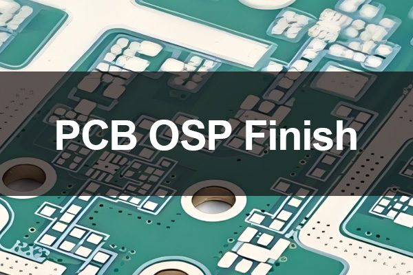
If you’re designing, sourcing, or manufacturing PCBs, PCB OSP finish is a critical choice that impacts performance, cost, and reliability across every electronic assembly step—and getting it right means avoiding costly reworks and failed production runs. PCB OSP finish has become a go-to for high-volume and high-precision electronics, but navigating its use, benefits, and limitations requires clear, technical clarity for every role in the PCB supply chain.
What Is PCB OSP Finish, and How Does It Work?
Core Definition of OSP Coating
OSP, or Organic Solderability Preservative, is a thin organic coating applied to bare copper PCB surfaces. It forms a protective layer that prevents copper oxidation during storage and processing.
The coating dissolves during soldering, exposing clean copper for strong, reliable solder joints without leaving residual material.
Key Chemical & Application Process
OSP coating uses azoles or triazoles as its active chemical components. Application is a wet process: clean copper PCBs are dipped in OSP solution, rinsed, and dried.
The resulting layer is just 0.5–2 μm thick, preserving PCB fine features and electrical conductivity.
What Are the Pros and Cons of PCB OSP Finish?
| Advantages of PCB OSP Finish | Disadvantages of PCB OSP Finish |
|---|---|
| Ultra-thin layer preserves fine-pitch (0.2mm+) PCB designs for high-density electronics | Limited shelf life (6–12 months) when stored in standard ambient conditions |
| No halogens or heavy metals—compliant with RoHS, REACH, and WEEE regulations | Sensitive to moisture and high humidity; oxidation risk if storage conditions are poor |
| Low cost vs. electroplated finishes (ENIG, Immersion Silver) | Not suitable for multiple reflow soldering cycles (best for 1–2 reflows only) |
| Smooth surface with no galvanic corrosion risk for copper substrates | Requires strict process control for soldering temperature and flux selection |
| Compatible with all standard solder pastes and assembly methods | No abrasion resistance; easy to scratch during handling and assembly |
How Does PCB OSP Finish Compare to Other PCB Surface Coatings?
| Coating Type | Key Use Case | Cost (vs. OSP) | Solderability | Shelf Life | Best For |
|---|---|---|---|---|---|
| PCB OSP Finish | High-volume, fine-pitch PCBs | Base (100%) | Excellent (1–2 reflows) | 6–12 months | Consumer electronics, automotive low-power PCBs |
| ENIG (Electroless Nickel Immersion Gold) | High-reliability, high-frequency PCBs | 300–400% higher | Superior (unlimited reflows) | 2+ years | Aerospace, medical electronics, servers |
| Immersion Silver | Mid-volume, general-purpose PCBs | 150–200% higher | Very good (2–3 reflows) | 12–18 months | Industrial control, LED lighting |
| Immersion Tin | High-density, lead-free assembly | 200–250% higher | Good (2 reflows) | 6–12 months | Communication equipment, power electronics |
| Hot Air Solder Leveling (HASL) | Low-cost, through-hole PCBs | 80–90% of OSP | Fair (1 reflow) | 12+ months | Basic industrial control, low-precision electronics |
Which Industries Benefit Most from PCB OSP Finish?
Consumer Electronics
PCB OSP finish is the top choice for smartphones, tablets, and wearables. Its thin layer supports 0.2mm fine-pitch components and high-density PCBs.
Low cost aligns with high-volume production, and RoHS compliance meets global consumer electronics regulations.
Automotive Electronics
For infotainment systems, sensor PCBs, and interior control modules, PCB OSP finish delivers reliable solder joints in moderate temperature environments.
It is ideal for high-volume automotive production and compatible with lead-free soldering standards for automotive manufacturing.
Communication Equipment
Routers, modems, and small cell PCBs use PCB OSP finish for its excellent electrical conductivity and fine-pitch compatibility.
The coating’s smooth surface minimizes signal loss in high-speed communication circuits at a lower cost than ENIG.
LED/Lighting
LED driver PCBs and panel light PCBs leverage PCB OSP finish for its low thermal resistance and compatibility with SMD LED assembly.
It supports high-volume production of lighting products and meets RoHS requirements for commercial and residential LED gear.
How to Ensure Proper Storage for PCB OSP Finish?
Proper storage is the single most important step to preserve PCB OSP finish solderability—failure here causes copper oxidation and soldering defects.
Store OSP-coated PCBs in sealed anti-static bags with desiccant and oxygen absorbers to control moisture and air exposure.
Maintain storage conditions at 15–25°C and relative humidity (RH) below 40%. Avoid temperature fluctuations and direct sunlight.
Label all PCB batches with production and expiration dates; use FIFO (First-In, First-Out) inventory management for OSP PCBs.
Do not open sealed bags until immediately before assembly. If bags are opened, use the PCBs within 72 hours in a controlled assembly environment (RH <50%).
If OSP PCBs are exposed to high humidity for over 72 hours, re-inspect for oxidation before soldering—discard if discoloration (tarnish) is visible.
What Soldering Processes Work Best with PCB OSP Finish?
PCB OSP finish pairs best with reflow soldering (infrared or convection) for SMD and fine-pitch components—wave soldering is possible but requires strict flux control.
Use no-clean or mild activated (MA) flux; aggressive fluxes are unnecessary and may leave residues that damage the OSP layer pre-soldering.
Set reflow soldering peak temperature to 240–250°C (lead-free) with a dwell time of 60–90 seconds above 217°C.
Avoid extended dwell times—high heat for too long degrades the OSP coating and increases oxidation risk.
For wave soldering, use a nitrogen-blanketed wave to reduce air exposure during soldering. Keep conveyor speed at 1.0–1.5 m/min for optimal coating dissolution.
After soldering, use only deionized water for cleaning (if needed); harsh chemicals will strip remaining OSP coating on unsoldered copper areas.
How to Detect Defects in PCB OSP Finish Before Assembly?
Visual inspection is the first step to identify PCB OSP finish defects—look for discoloration (brown/black tarnish), scratches, or uneven coating on copper surfaces.
Tarnish indicates oxidation and means the OSP layer has failed; scratched coating exposes bare copper to further oxidation.
Use a solderability test (dip test) for quantitative verification: dip a small section of the PCB in molten solder at 235°C for 2 seconds.
Clean copper should show 100% solder wetting; poor wetting (beading) means the OSP finish is non-functional and the PCB is unfit for assembly.
Check for coating thickness with a profilometer—target 0.5–2 μm; thickness above 2 μm causes soldering delays and poor joint formation.
Thickness below 0.5 μm means the coating is too thin to prevent oxidation during storage and processing.
What Design Considerations Apply to PCB OSP Finish?
For fine-pitch PCBs (pitch ≤0.3mm), PCB OSP finish is the optimal choice—its thin layer does not add bulk to pad surfaces.
Avoid sharp copper pad edges; round edges (radius ≥0.1mm) prevent OSP coating thinning and oxidation at stress points.
Ensure copper pad surfaces are smooth (Ra ≤0.8 μm) before OSP application—rough surfaces trap air and cause uneven coating.
Minimize the number of copper-to-copper gaps in fine-pitch areas; these gaps increase the risk of coating voids.
For double-sided PCBs, apply OSP coating to both sides in a single process to ensure consistency.
Avoid using OSP finish on PCBs that require multiple rework or reflow cycles—design these PCBs with ENIG or immersion silver instead.
What Are the Top PCB OSP Finish Search Questions?
Can PCB OSP finish be used for lead-free soldering?
Yes, PCB OSP finish is fully compatible with all lead-free solder pastes (Sn-Cu, Sn-Ag-Cu, Sn-Zn) and lead-free soldering processes.
Its organic coating dissolves at lead-free soldering temperatures (240–250°C) to create strong solder joints with no lead-based residues.
How long is PCB OSP finish solderable after opening the bag?
Once the sealed anti-static bag is opened, PCB OSP finish remains solderable for 72 hours in a controlled assembly environment (RH <50%, 15–25°C).
After 72 hours, copper oxidation begins, and solder wetting performance degrades significantly.
Is PCB OSP finish compatible with conformal coating?
Yes, PCB OSP finish is compatible with all standard conformal coatings (acrylic, epoxy, silicone, urethane).
The clean copper surface (after soldering) provides excellent adhesion for conformal coatings, with no OSP residues to interfere with bonding.
Can PCB OSP finish be used on flexible PCBs (FPC)?
Yes, PCB OSP finish works for flexible PCBs and flex-rigid PCBs—its thin, flexible coating moves with the FPC without cracking or peeling.
It is ideal for high-volume FPC production in consumer electronics and wearables due to its low cost and fine-pitch support.
F A Q
FAQ: Common Problems with PCB OSP Finish (and Solutions)
Q: Why is my PCB OSP finish showing brown tarnish after storage?
A: Brown tarnish on PCB OSP finish is caused by copper oxidation, usually from poor storage conditions (high humidity, open bags, or expired shelf life). Dispose of tarnished PCBs—oxidation cannot be reversed, and soldering will fail. Prevent this by storing OSP PCBs in sealed bags with desiccant and oxygen absorbers at RH <40%.
Q: Why is solder beading on OSP-coated PCB pads during reflow?
A: Solder beading is a sign of poor solder wetting, caused by either oxidized OSP finish or incorrect flux selection. First, verify the PCB is within its shelf life and was stored properly. If the PCB is good, switch to a mild activated (MA) no-clean flux—aggressive fluxes are not needed, but non-activated fluxes will not dissolve the OSP layer fully.
Q: Can I rework a PCB with OSP finish after soldering?
A: Limited rework is possible for PCB OSP finish—one minor rework (reflow) is acceptable if done within 24 hours of the original soldering. Multiple reworks cause the OSP coating to degrade completely, exposing copper to oxidation and leading to poor resoldering results. For PCBs that need frequent rework, choose ENIG instead of OSP finish.
Q: Why is the OSP coating peeling off my PCB during handling?
A: OSP coating peeling is caused by either a thin coating (≤0.5 μm) or rough copper pad surfaces (Ra >0.8 μm) before application. Ensure your PCB supplier applies OSP coating to a thickness of 0.5–2 μm and polishes copper pads to a smooth finish (Ra ≤0.8 μm). Also, use anti-static gloves for all PCB handling—oil from bare hands damages the OSP layer.
Q: Is PCB OSP finish suitable for high-temperature automotive PCBs?
A: PCB OSP finish is not recommended for automotive PCBs in high-temperature environments (e.g., engine bay, exhaust systems) where temperatures exceed 85°C for extended periods. The organic coating degrades at high temperatures, leading to copper oxidation. For high-temperature automotive PCBs, use ENIG or immersion silver—these finishes have better thermal stability.
Q: Why do my OSP-coated PCBs have poor solder joints on fine-pitch pads?
A: Poor solder joints on fine-pitch pads are usually caused by OSP coating thickness above 2 μm or incorrect reflow temperature. The thick OSP layer takes longer to dissolve, leading to incomplete wetting on small fine-pitch pads. Ensure the OSP coating is 0.5–2 μm and set the reflow peak temperature to 245–250°C with a 70–90 second dwell above 217°C.
How to Select a Reliable PCB OSP Finish Supplier?
Choose a supplier with ISO 9001 and IATF 16949 certifications—these standards ensure strict process control for OSP coating application.
Verify the supplier has in-house coating thickness and solderability testing to guarantee consistent OSP finish quality.
Ask for industry-specific case studies (consumer electronics, automotive, communication) to confirm the supplier’s experience with PCB OSP finish.
Ensure the supplier offers custom OSP coating options (thickness, chemical formulation) for your specific PCB design and assembly needs.
Check the supplier’s lead times and inventory capabilities—reliable suppliers can meet high-volume production demands for OSP-coated PCBs.
Request a sample batch of OSP-coated PCBs to test solderability, storage stability, and defect rates before placing a full order.
How to Optimize PCB OSP Finish for High-Volume Production?
Standardize PCB OSP finish specifications with your supplier (0.5–2 μm thickness, RoHS-compliant formulation) to eliminate variability.
Implement FIFO inventory management for OSP PCBs to ensure no expired material is used in production.
Integrate pre-assembly OSP finish inspection (visual + solderability test) into your production line to catch defects early and reduce reworks.
Optimize your soldering process for OSP—use MA no-clean flux and standardize reflow/wave soldering parameters to avoid coating degradation.
Work with your PCB supplier to implement a sealed packaging system (desiccant + oxygen absorbers) tailored to your production lead times.
Train your assembly team on proper OSP PCB handling (anti-static gloves, controlled environment) to prevent scratches and oxidation.
At Thindry, we specialize in high-quality PCB OSP finish for consumer electronics, automotive electronics, communication equipment, and LED/lighting industries—our strict process control and industry-specific expertise ensure your OSP-coated PCBs deliver consistent solderability, reliability, and performance across every production run. Whether you need high-volume standard OSP PCBs or custom fine-pitch OSP designs, our team of PCB engineers will work with you to meet your exact specifications and assembly needs. For all your PCB OSP finish orders and technical inquiries, send an email to sales@pcbtry.com—we’re ready to support your PCB production and assembly goals with top-tier OSP coating solutions.


0 Comments