
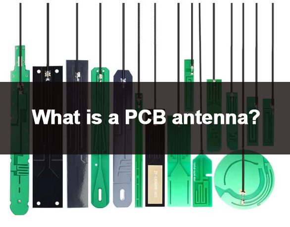
A PCB antenna is a small antenna made by etching copper foil or other conductive material into specific patterns on a printed circuit board (PCB). Its job is to send and receive wireless signals. Unlike external antennas that need to be added separately, a PCB antenna is built directly into the PCB—this cuts out extra assembly steps and makes devices smaller. This guide covers everything you need to know about PCB antennas, from the basics to real-world uses, common problems, and how to fix them.
What is a PCB Antenna and How Does It Work?
A PCB antenna is a passive component (it doesn’t need extra power) that converts electrical signals into electromagnetic waves (to send signals) and vice versa (to receive signals). Here’s how it works: when electricity flows through the etched copper pattern, it creates changing electric and magnetic fields that travel as wireless signals.
Most PCB antennas use a quarter-wavelength (λ/4) design—this means the copper trace length is one-fourth the length of the signal it’s meant to handle. You can calculate the trace length easily with this simple formula: λ (mm) = 300 / frequency (GHz). For example, for a 2.4GHz signal: 300 ÷ 2.4 = 125mm, so one-fourth of that is 31.25mm (round to ~31mm). The PCB’s ground plane acts like a mirror for the trace, forming a complete structure that boosts signal strength—just make sure the ground plane is solid (no gaps) for the best results.
What Are the Main Types of PCB Antennas?
There are several types of PCB antennas, each designed for specific signal frequencies and uses. The most common ones are listed below, with simple explanations:
- Microstrip Antenna: A flat, compact design with a metal patch on one side of the PCB and a ground plane on the other. It works well for 2.4GHz, 5GHz, and 5G (sub-6GHz) signals, which are common in smartphones and tablets. Quick tip: Keep the metal patch size in line with the signal’s wavelength to avoid losing signal strength.
- PIFA (Planar Inverted-F Antenna): Has a shorted pin and folded copper trace, making it easier to tune to the standard 50Ω impedance and smaller than microstrip antennas. It’s commonly used in smartphones and wearables—its folded design saves 20-30% of PCB space compared to microstrip antennas.
- Monopole Antenna: A single copper trace paired with a ground plane. It’s simple to design and cheap to make, making it perfect for low-frequency IoT devices (like LoRa sensors) and industrial sensors. Pro tip: The bigger the ground plane, the better the signal range.
- Loop Antenna: A circular or rectangular copper trace, great for low-frequency uses like RFID, NFC (13.56MHz), and access control. It’s resistant to interference, which is ideal for smart cards. Quick tip: The loop’s diameter should be about one-tenth the signal’s wavelength for best performance.
How Does a PCB Antenna Compare to External Antennas?
Deciding between a PCB antenna and an external antenna depends on your device’s size, cost, and how well it needs to perform. The table below breaks down the key differences in simple terms:
| Feature | PCB Antenna | External Antenna |
|---|---|---|
| Size & Integration | Integrated with PCB, ultra-compact, saves device space (critical for wearables/IoT) | Requires extra space, needs assembly, increases device size (not ideal for small devices) |
| Cost | Low cost, no additional components or assembly fees (reduces BOM cost by 15-20%) | Higher cost, includes antenna component and assembly (adds $0.5-$2 per unit) |
| Performance | Good for short-to-medium range (10-100m); affected by PCB layout and interference (fix with proper ground plane) | Better long-range performance (100m+); less affected by device internal interference (best for routers/base stations) |
| Installation | No extra installation; fabricated during PCB production (saves assembly time) | Requires manual assembly, may need wiring or connectors (adds production time) |
| Application | Small devices (smartphones, wearables, IoT sensors) where space is critical | Large devices (routers, base stations, industrial equipment) where range is priority |
What Are the Key Design Factors for a High-Performance PCB Antenna?
To design a PCB antenna that works well, you need to pay attention to a few key factors—these directly affect how strong the signal is, how efficient the antenna is, and how reliable it is. Ignore them, and you’ll likely run into performance issues.
1. Trace Length and Shape
The copper trace’s length must match the signal’s wavelength (usually one-fourth or one-half of the wavelength). Use this simple formula: λ (mm) = 300 / frequency (GHz). For example, a 2.4GHz PCB antenna needs a trace length of ~31mm (300 ÷ (2.4 × 4) = 31.25mm).
If you’re short on PCB space, use snake-shaped traces—they reduce the amount of space needed without changing the trace’s effective length. Pro tip: Make snake bends at 45° (not 90°) to avoid signal reflection and loss.
2. Ground Plane Design
A solid ground plane is a must for a good PCB antenna. It acts as a reference point for the antenna, reduces signal loss, and makes the antenna more efficient at radiating signals.
The ground plane should be at least 1.5 times the size of the antenna and free of gaps or cuts near the antenna trace. Don’t route signal traces or place vias (small holes that connect PCB layers) near the antenna on the ground plane—these create “holes” that weaken performance.
3. Substrate Material
The PCB’s substrate (the base material) affects how much signal is lost and the antenna’s impedance (signal resistance). Choose low-loss materials: FR-4 (dielectric constant ~4.4) is common for consumer electronics, while PTFE (dielectric constant ~2.1) works best for high-frequency 5G/6G signals. Use FR-4 for 2.4/5GHz; switch to PTFE for frequencies above 10GHz.
The substrate’s thickness and dielectric constant (a measure of how well it stores electrical energy) also matter—thicker substrates with lower dielectric constants reduce signal loss.
4. Clearance (Keep-Out Area)
The PCB antenna needs a clear area (called a keep-out zone) with no other components—especially metal parts. Metal near the antenna can block or reflect signals, making it less efficient.
We recommend a minimum of 5-10mm between the PCB antenna and other components for best performance. For metal components (like batteries or connectors), increase that distance to 10-15mm to avoid blocking signals.
How Are PCB Antennas Used in Key Industries? (4 Real-World Cases)
PCB antennas are used in many industries because they’re small, cheap, and easy to integrate. Below are four common industries with real-world examples, so you can see how they’re used in practice:
1. Consumer Electronics
Smartphones and smartwatches use PCB antennas (PIFA type) for Wi-Fi, Bluetooth, and GPS. For example, a smartwatch uses a small PIFA PCB antenna (8×12mm) to enable Bluetooth 5.2 connectivity—this keeps the watch small enough to wear on your wrist.
This design solves the problem of limited space in wearables while still providing reliable wireless communication for fitness tracking and notifications.
2. Automotive Electronics
New energy vehicles use PCB antennas in their T-Box modules (the device that connects the car to the internet) for GPS, 4G/5G, and V2X (car-to-car/car-to-infrastructure) communication. One of our automotive clients used our custom PCB antenna (15×20mm) to cut PCB area by 30% while supporting global signal bands (850/900/1800/1900MHz).
This antenna can handle high temperatures and vibrations, solving the problem of reliable communication in the harsh environment of a car.
3. Industrial Control/Automation
Warehouse IoT sensors use PCB antennas (monopole type) for LPWAN (LoRa) communication (long-range, low-power signals). Our custom monopole PCB antenna works reliably even inside metal enclosures—signal efficiency only drops by 5% (compared to 20-30% for standard antennas).
This solves the problem of metal enclosures blocking signals, allowing real-time inventory and environmental monitoring in warehouses.
4. Communication Devices
Wi-Fi 7 routers use PCB antennas (microstrip type) to support multi-band signals (2.4GHz, 5GHz, 6GHz). This antenna has a high efficiency (up to 80%), ensuring fast data transfer speeds (up to 5.8Gbps) and wide coverage (up to 150m).
This meets the need for fast, reliable wireless in modern homes and offices, where multiple devices (phones, laptops, smart TVs) connect at the same time.
What Are Common PCB Antenna Problems and How to Fix Them?
Many people run into performance issues with PCB antennas, usually because of poor design or installation. Below are simple, practical solutions to the most common problems:
1. Weak Signal Strength
Weak signals are usually caused by a trace that’s too short, a small ground plane, or interference. Fix this by adjusting the trace length to match the target frequency (use the λ/4 formula) and making the ground plane bigger.
Move the antenna away from metal components and make sure it has a clear keep-out area to reduce interference.
2. Impedance Mismatch
Impedance mismatch (the ideal is 50Ω for most uses) causes signal loss and poor efficiency. Use a network analyzer to test impedance; make the trace wider (wider = lower impedance) or add small components (like 0402 capacitors/inductors) to tune it to 50Ω.
3. Interference from Other Components
Components like power supplies and microcontrollers can interfere with PCB antenna signals. Keep the antenna at least 10mm away from these high-noise components and use a ground plane divider to block interference.
4. Poor Performance in Metal Enclosures
Metal enclosures reflect signals, making the antenna less efficient. Move the PCB antenna 10mm away from the enclosure walls, or use a high-dielectric substrate (like Rogers 4350) to improve signal penetration by 15-20%.
FAQ: Common Questions About PCB Antennas
1. Can a PCB Antenna Work for 5G and 6G Applications?
Yes, PCB antennas work for 5G and 6G. Use low-loss substrates (like PTFE or Rogers 5880) and optimize the trace design (e.g., coplanar waveguide), and they can support frequencies up to 30GHz and higher. Many 5G smartphones use PCB antennas for mmWave communication (28GHz/39GHz) with a signal gain of up to 8dBi (higher dBi = better range).
2. Do PCB Antennas Require Special PCB Manufacturing Processes?
No, most PCB antennas can be made using standard PCB manufacturing processes. The only requirement is precise etching of the copper trace to get the correct length and shape (tolerance ±0.1mm). For high-frequency signals (above 10GHz), use high-precision etching and controlled impedance (50Ω) to avoid signal degradation.
3. How to Test the Performance of a PCB Antenna?
Use a network analyzer to test key performance metrics: return loss (target: <-15dB; lower = better), gain (measured in dBi; higher = better range), and bandwidth (should cover your target frequency). For real-world testing, measure signal range and reliability in the environment where the device will be used (e.g., warehouse, office) to make sure it works as needed.
4. Can PCB Antennas Be Customized for Specific Applications?
Yes, PCB antennas can be fully customized for frequency, size, and performance. We specialize in custom PCB antenna design, tailored to your device’s needs—support on-demand customization + free DFM report to ensure the antenna is easy to manufacture and performs well.
5. Are PCB Antennas Suitable for Low-Power IoT Devices?
Absolutely. PCB antennas are low-power and energy-efficient, making them perfect for low-power IoT devices like sensors and wearables. Their small size fits the compact design of most IoT devices, while still providing reliable short-range communication.
6. What Is the Typical Range of a PCB Antenna?
Range depends on frequency and design, but most PCB antennas have a range of 10-100 meters for short-range uses (Wi-Fi, Bluetooth). For long-range IoT applications (LPWAN, LoRa), the range can reach 2-5 kilometers with an optimized design (low frequency + high gain).
How to Choose the Right PCB Antenna for Your Project?
Choosing the right PCB antenna starts with figuring out what your project needs. Follow these simple steps to make the right choice:
- Define the target frequency (e.g., 2.4GHz for Bluetooth, 5G for mobile communication).
- Determine the device size and available PCB space—this will dictate the antenna type (e.g., PIFA for small devices).
- Consider the communication range (short vs. long-range) and required gain.
- Evaluate the operating environment (e.g., metal enclosures, high temperatures) to select the right substrate and design.
- Work with a trusted manufacturer to ensure custom design and quality production—we offer tailored PCB antenna solutions with free DFM reports, including layout checks and performance simulations, to avoid problems during manufacturing.
Why Choose Thindry for Your PCB Antenna Needs?
At Thindry, we specialize in high-quality PCB antenna design and manufacturing, with years of experience serving the consumer electronics, automotive, industrial, and communication industries. We offer custom solutions to meet your unique needs—including tuning the frequency, optimizing size, and reducing interference—with a focus on performance, reliability, and cost-effectiveness.
We provide PCB antenna products, support on-demand customization + free DFM report, and ensure strict quality control to meet industry standards. If you need a reliable PCB antenna for your project, contact us to place an order at sales@pcbtry.com.


0 Comments