
Core Concepts & Importance
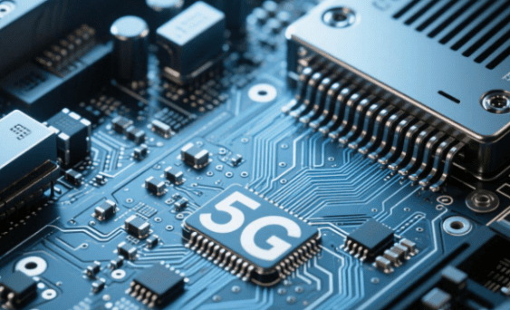
The Printed Circuit Board (PCB), serving as the support structure for electronic components and the provider of electrical connections, is hailed as the “Mother of Electronic Products.” In the 5G era, 5G communication PCBs are not merely simple connectors but are critical foundations enabling high-frequency, high-speed signal transmission. Designed specifically for fifth-generation mobile networks, they differ significantly from traditional PCBs in materials, design, manufacturing processes, and testing standards to meet 5G’s stringent demands for high frequency, high speed, low latency, and high reliability.
Compared to 4G, 5G offers a 10-20x increase in transmission rate and reduces latency to below 1 millisecond. These leaps present unprecedented challenges for PCBs. Operating frequencies have shifted from below 3GHz to 6GHz and even millimeter-wave bands (24-30GHz), leading to more significant signal attenuation and loss. Consequently, 5G communication PCBs must adopt entirely new material systems, design concepts, and manufacturing processes to ensure signal integrity and stability.
With accelerating global 5G deployment, the 5G communication PCB market is experiencing explosive growth. Prismark predicts the global PCB output value will reach $96.8 billion in 2023, with 5G-related PCBs being one of the fastest-growing segments. China, as the world’s largest PCB manufacturing base accounting for over 50% of global output, holds a pivotal position in this field. The table below compares key parameters of 5G communication PCBs versus traditional PCBs:
Table: Key Parameter Comparison: 5G Communication PCBs vs. Traditional PCBs
| Parameter | Traditional PCB | 5G Communication PCB | Key Improvement |
|---|---|---|---|
| Signal Rate | 1-10 Gbps | >10-20 Gbps | 10-20x Increase |
| Impedance Tolerance | ±10% | ±5% to ±8% | ~2x Tighter |
| Line Width Tolerance | ±20% | ≤ ±10% | 2x Tighter |
| Dielectric Thickness Uniformity | Not Strict | ≤15% | Extreme Consistency Required |
| Operating Frequency | < 3GHz | Up to 30GHz (mmWave) | Significant Increase |
| Thermal Management | Standard | High Tc Materials, RTI 150°C | Greatly Enhanced |
5G communication PCBs form the physical foundation of 5G technology, their performance directly determining network coverage, speed, and signal quality. As experts note, “In the 5G era, PCBs are no longer just connectors but are core carriers for signals, power, and interconnects – the ‘hardware cornerstone’ of 5G implementation.”
Core Characteristics of 5G Communication PCBs
The distinguishing characteristics of 5G communication PCBs compared to traditional PCBs are mainly reflected in three aspects: high-frequency and high-speed transmission capability, high-density integration characteristics, and unique thermal management requirements. These characteristics have led to revolutionary changes in the design, materials, and manufacturing processes of 5G communication PCBs.
High-Frequency and High-Speed Characteristics
5G communication operates in higher frequency bands, with Sub-6GHz and millimeter-wave bands (24GHz-52GHz) becoming mainstream, placing extremely high demands on the high-frequency performance of PCBs. High-frequency signal transmission leads to a pronounced “skin effect,” where current concentrates on the conductor surface, making copper foil roughness a key factor affecting signal loss. To reduce transmission loss, 5G communication PCBs must use low-roughness copper foil (Ra < 0.5μm) to minimize signal loss caused by impedance anomalies.
In terms of high-speed characteristics, the data signal transmission rate of 5G products increases from 25Gbps to 56Gbps or even higher. This high-speed transmission requires PCBs to have strict impedance control (tolerance improved from ±10% to ±5%) and extremely low signal loss. To achieve this goal, 5G communication PCBs typically use special materials with low dielectric constant (Dk) and low dissipation factor (Df), such as Polytetrafluoroethylene (PTFE), Liquid Crystal Polymer (LCP), and ceramic-filled composite materials.
High-Density Integration Characteristics
The functional complexity of 5G equipment requires PCBs to accommodate more components and more complex circuit designs. High-Density Interconnect (HDI) technology has become one of the core technologies for 5G communication PCBs, enabling more connections in a smaller space through microvias, blind vias, and buried vias. Any-layer HDI technology allows connections between any layers of the PCB, greatly enhancing design flexibility and signal transmission efficiency.
The direct challenge brought by high-density integration is electromagnetic interference and thermal management issues. 5G equipment widely uses Multiple-Input Multiple-Output (MIMO) technology, integrating multiple Antenna Array Units (AAUs), which makes electromagnetic interference, crosstalk, and parasitic capacitance key issues in 5G RF PCB design. To address these problems, 5G communication PCBs require finer line layout, reasonable shielding design, and strict impedance matching techniques.
Thermal Management Characteristics
5G equipment generates significant heat during operation, primarily stemming from high-frequency, high-speed signal transmission and high-power requirements. China’s initial commercial 5G frequency bands are mainly below 6GHz, later reaching 24-30GHz. With continuously increasing transmission rates, data transmission volume greatly increases, leading to a significant rise in the heat generation capability of 5G communication terminals compared to the 4G era.
Efficient thermal management has become a key challenge in 5G communication PCB design. On one hand, PCBs need to use high thermal conductivity materials (higher Tc requirement) to improve heat dissipation efficiency; on the other hand, thermal design optimization (such as embedded copper blocks, adding thermal vias, etc.) is needed to enhance heat dissipation capability. Simulation studies show that high thermal conductivity (Tc) is more effective than reducing the material’s Df value for lowering temperature rise. Therefore, the Relative Thermal Index (RTI) of 5G communication PCB laminates has been upgraded from 105°C to 150°C.
Table: Performance Comparison of Major High-Frequency Materials for 5G Communication PCBs
| Material Type | Dielectric Constant (Dk) | Dissipation Factor (Df) | Thermal Stability | Applicable Scenarios |
|---|---|---|---|---|
| PTFE | ~2.2 | 0.001-0.002 | Good | Base station antennas, RF circuits |
| LCP | 2.5-3.2 | 0.002-0.0045 | Excellent | Flexible circuits, high-frequency microstrip lines |
| Hydrocarbon Resin | ≈2.4 | ≈0.0002 | High heat resistance | Base station power amplifiers |
| PPE/PPO | 2.5-3.5 | 0.001-0.002 | Good water resistance | Various high-frequency applications |
Key Design Challenges for 5G Communication PCBs
The design of 5G communication PCBs is a complex engineering task encompassing multidisciplinary knowledge such as materials science, electromagnetics, and thermodynamics, facing various technical challenges. These challenges mainly stem from the stringent requirements of 5G technology for high-frequency and high-speed signal transmission, as well as the development trend towards equipment miniaturization and high integration.
Signal Integrity Challenges
In the 5G high-frequency and high-speed environment, signal integrity becomes a core challenge in PCB design. As signal frequency increases and transmission rates accelerate, issues of signal attenuation, reflection, and distortion become particularly prominent. The data signal transmission rate of 5G products increases significantly from 25Gbps to 56Gbps, placing extremely stringent requirements on product impedance, loss, etc.
Signal integrity challenges mainly come from the following aspects: Firstly, impedance matching becomes critically important. 5G communication PCBs require impedance tolerance control within ±5%, far stricter than the ±10% requirement for traditional PCBs. Minor impedance discontinuities can cause signal reflection, reducing transmission quality. Secondly, transmission loss control becomes more difficult. Dielectric loss and conductor loss in high-frequency signal transmission increase significantly with rising frequency, requiring optimization through precise electromagnetic simulation and material selection. Thirdly, timing synchronization requirements are higher. 5G high-speed signals are extremely sensitive to transmission delay, requiring highly consistent transmission times for signals across different paths on the PCB.
To address these challenges, PCB designers need to use advanced electromagnetic simulation software to predict and optimize signal integrity during the design phase. Simultaneously, precise microstrip line design techniques are needed to strictly match the characteristic impedance to the 50Ω standard. For example, in the 28GHz frequency band, the microstrip line width needs to be precisely controlled between 0.1-0.2mm to avoid signal reflection. Additionally, vias need to use back-drilling technology to remove excess stub, and corners should use 45° or arc transitions instead of right angles to maintain impedance continuity.
Electromagnetic Compatibility Challenges
5G equipment contains numerous internal components with compact layouts, prone to Electromagnetic Interference (EMI) and Electromagnetic Susceptibility (EMS) problems. Especially in applications using Massive MIMO technology, where multiple antenna units operate simultaneously, Electromagnetic Compatibility (EMC) design becomes particularly critical.
EMC challenges are mainly manifested in three aspects: first, crosstalk problems, i.e., mutual interference between different signal lines, which intensifies with increasing line density; second, radiation interference, where high-frequency signals generate electromagnetic radiation, affecting the operation of surrounding circuits; third, external interference, as 5G equipment needs to maintain stable operation in complex electromagnetic environments, requiring higher capability to suppress external interference.
Addressing EMC challenges requires comprehensive measures. In terms of layout, it is necessary to reasonably arrange the positions of different functional circuits, ensuring sufficient isolation between high-power circuits and low-noise circuits. In terms of circuit design, appropriate shielding layers and filters need to be added, and reasonable grounding strategies should be adopted to reduce EMI impact. Furthermore, for particularly sensitive RF circuits, multi-layer shielding structures may be required to provide additional protection.
Thermal Management Challenges
The high-power operation of 5G equipment generates substantial heat, making thermal management a key challenge in PCB design. High-speed signals generate significant heat; if heat dissipation is insufficient, it can lead to issues like copper wire peeling, delamination, and board warping, significantly reducing PCB performance and lifespan.
Thermal management challenges are mainly reflected in two aspects: first, increased power density, as 5G equipment integrates more functions into a smaller space, significantly increasing power density; second, high-temperature sensitivity, as 5G high-frequency and high-speed signals are more sensitive to temperature changes, and temperature fluctuations can affect signal transmission stability.
To address thermal management challenges, 5G communication PCBs need to start from both material selection and structural design. Material-wise, it is necessary to select substrate materials with high thermal conductivity, such as special resin materials with higher thermal conductivity (Tc). Research indicates that high thermal conductivity (Tc) is more effective than reducing the material’s Df value for lowering temperature rise. Design-wise, active cooling technologies such as thermal vias and embedded copper blocks need to be adopted, along with reasonable thermal distribution design to avoid local heat accumulation.
The Material Revolution in 5G Communication PCBs
The performance improvement of 5G communication PCBs largely benefits from breakthroughs in materials science. To meet the requirements of high-frequency and high-speed signal transmission, traditional PCB materials are gradually being replaced by new high-performance materials. This material revolution covers the entire material system, including substrates, copper foil, inks, etc.
Innovations in High-Frequency Substrate Materials
Substrate materials are the core component of PCBs and play a decisive role in signal transmission performance. The high-frequency characteristics of 5G communication require substrate materials to have lower Dielectric Constant (Dk) and Dissipation Factor (Df) to reduce energy loss during signal transmission. Currently, the main types of high-frequency substrate materials suitable for 5G communication PCBs are as follows:
Polytetrafluoroethylene (PTFE) is one of the earliest substrate materials applied in high-frequency circuits, with very low Dk (~2.2) and Df (0.001-0.002) values. PTFE material has good chemical stability and high-temperature resistance, but its coefficient of thermal expansion is large and thermal conductivity is poor, requiring enhancement modification by adding ceramics or glass fiber. Modified PTFE composite materials significantly improve mechanical strength and thermal stability while maintaining excellent high-frequency performance.
Liquid Crystal Polymer (LCP) is a new high-frequency material receiving much attention in the 5G era. Depending on formation conditions, LCP can be divided into two categories: thermotropic liquid crystals that melt upon heating and lyotropic liquid crystals dissolved by solvents. LCP materials have low moisture absorption, high heat resistance, and excellent high-frequency performance, making them particularly suitable for flexible PCBs and millimeter-wave band applications. Based on molecular structure, LCP can be divided into Type I, II, and III, with decreasing heat resistance, meeting the needs of different application scenarios.
Hydrocarbon resin materials are another important category of high-frequency substrate materials, such as butadiene-styrene copolymer, butadiene homopolymer, etc. The Dk value of these materials is about 2.4, and the Df value is as low as 0.0002, possessing excellent dielectric properties and high heat resistance. The disadvantage is poor adhesion, requiring surface treatment or additives to improve bonding strength with copper foil.
New Copper Foils and Conductive Materials
The “skin effect” in 5G high-frequency signal transmission makes the surface roughness of copper foil extremely critical to signal loss. Traditional PCBs use copper foil with relatively high surface roughness, leading to significant signal loss. 5G communication PCBs must use low-profile copper foil, whose surface roughness (Ra) needs to be controlled below 0.5μm.
To meet this requirement, copper foil manufacturers have developed new copper foil products such as ultra-flat copper foil and reverse-treated copper foil. These coppers achieve a significant reduction in surface roughness through special electrolytic processes and treatment technologies. Simultaneously, the purity of copper foil has been improved, reducing the impact of impurities on signal transmission.
Besides the improvement in copper foil performance itself, 5G communication PCBs also adopt new surface treatment technologies. Traditional solder mask inks have become a bottleneck for high-frequency signal transmission, making the research and application of ultra-low loss inks urgent. Meanwhile, to reduce the impact of the skin effect at high frequencies, the application of low-roughness oxide treatment chemicals in high-speed board processing is becoming increasingly widespread.
Special Materials and Applications
The diverse application scenarios of 5G communication have driven the development of a series of special materials. For example, polyimide materials for adhesive-less flexible copper clad laminates for flexible electronic devices require low dielectric constant (Dk ≤ 3.2) and low loss characteristics (Df ≤ 0.005), while also meeting mechanical performance requirements such as high peel strength (≥ 1.0 N/mm) and low water absorption (≤ 0.8%).
In high-power application scenarios, such as 5G base station power amplifiers, the requirements for PCB heat dissipation performance are extremely high, necessitating the use of high thermal conductivity ceramic-filled materials or metal-based composite materials. These materials maintain excellent high-frequency characteristics while possessing outstanding thermal management capabilities, meeting the heat dissipation needs of high-power operation in 5G equipment.
As 5G technology develops towards higher frequency bands, packaging substrate materials also face new challenges. Packaging substrate materials based on Ajinomoto Build-up Film (ABF) show unique advantages in the 5G millimeter-wave band, whose excellent flatness and high-frequency performance meet the stringent requirements for chip-level interconnects.
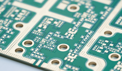
Process Innovations for 5G Communication PCBs
The manufacturing processes for 5G communication PCBs differ significantly from traditional PCBs. These process innovations are the technical guarantee for achieving the high-performance requirements of 5G. From drilling and circuit formation to inspection and testing, the entire manufacturing流程 has undergone technological革新 to meet the stringent requirements of 5G communication PCBs for precision, reliability, and consistency.
Fine Line Processing Technology
The line fineness requirements for 5G communication PCBs are far higher than those for traditional PCBs, with line width tolerance improved from ±20% to within ±10%, pushing traditional subtractive processes to their limits. To meet higher precision requirements, PCB manufacturers are turning to improved Semi-Additive Process (MSAP), which can form finer lines and achieve stricter tolerance control.
The MSAP process first applies a thin copper layer on the laminate without photoresist, then forms the circuit pattern through special lithography technology, and the copper existing between conductors is further etched away. The key advantage of the MSAP process is its ability to achieve high-precision etch control, thereby reducing signal loss caused by impedance anomalies. This process is particularly suitable for producing the fine lines required for 5G millimeter-wave bands.
In drilling technology, 5G communication PCBs require smaller microvias and higher hole position accuracy, which traditional mechanical drilling can hardly meet. Laser drilling technology has become the mainstream technology for microvia processing in 5G communication PCBs, enabling the production of smaller microvias (≤ 50μm) and higher hole position accuracy. Simultaneously, to meet Any-layer HDI requirements, laser drilling technology is combined with plating and via filling processes to achieve reliable manufacturing of high-density interconnect structures.
High-Density Interconnect Technology
The demand for miniaturization and high performance in 5G equipment has driven the rapid development of High-Density Interconnect (HDI) technology. HDI PCBs achieve more complex circuit designs and higher wiring density through microvias, blind vias, and buried vias. 5G communication PCBs commonly use multi-step HDI designs, even any-order interconnect technology, to meet the requirements of extremely high-density wiring.
The core challenge of high-density interconnect technology is ensuring interlayer alignment accuracy and interconnection reliability. As the number of PCB layers increases (5G base station PCBs can have over 20 layers), interlayer alignment accuracy needs to be controlled within ±20μm, placing extremely high demands on lamination processes and material stability. To address this challenge, PCB manufacturers adopt high-precision alignment systems and stable lamination processes to ensure precise interlayer alignment in multi-layer boards.
Another important technology is back drilling, used to reduce the impact of via stub on high-speed signals. In products with rates of 112G and above, the stub effect becomes non-negligible, and back drilling places stricter requirements on stub, with zero-stub technology becoming a trend. Back drilling technology removes the unnecessary metallized part of the via through secondary drilling, reducing signal reflection and distortion, and improving signal integrity.
Advanced Inspection and Testing Technologies
The high-precision requirements of 5G communication PCBs must be matched with advanced inspection and testing technologies to ensure product quality and reliability. Traditional visual inspection and electrical testing can no longer meet the requirements of 5G communication PCBs, necessitating the introduction of more precise inspection methods.
Automated Optical Inspection (AOI) systems play a key role in the manufacturing of 5G communication PCBs. Advanced AOI systems identify potential faults by measuring the conductivity of top and bottom signal lines in through-holes or assembly, improving fault detection accuracy, reducing false positives, and shortening production line delays. AOI systems integrated with Artificial Intelligence (AI) can independently learn and optimize detection algorithms, further improving inspection accuracy and efficiency.
For the electrical performance testing of 5G communication PCBs, specialized high-frequency testing methods are required. Vector Network Analyzers can be used to perform full-frequency band sweeps on PCBs, accurately measuring key indicators such as Voltage Standing Wave Ratio (VSWR), return loss, and insertion loss. Simultaneously, reliability testing under different temperature and humidity environments is necessary to ensure PCB performance stability under complex working conditions.
Furthermore, X-ray inspection technology also plays an important role in the inspection of 5G communication PCBs. X-ray technology utilizes the difference in X-ray absorption rates of different substances to detect internal defects, making it particularly suitable for inspecting ultra-fine pitch, ultra-high-density circuit boards. This non-destructive testing method can detect hidden defects such as inner layer line breaks and incomplete hole metallization.
Application Areas of 5G Communication PCBs
As the hardware foundation of 5G technology, 5G communication PCBs find applications across the entire 5G ecosystem, from infrastructure to terminal equipment. With the accelerated deployment of 5G technology worldwide, 5G communication PCBs are showing huge market demand and growth potential in several key areas.
5G Base Station Construction
5G network construction has brought a substantial increase in the volume of base station PCBs. Compared to 4G base stations, 5G base stations not only increase significantly in quantity (estimated to be over 10 times that of 4G base stations) but also see a significant rise in the value of PCBs per individual base station (approximately more than twice that of 4G base stations). This trend of “volume and price rising together” brings huge growth space for the 5G communication PCB market.
Changes in the structure of 5G base stations place new demands on PCBs. The application of Massive MIMO technology requires larger area and more layered PCBs for the Active Antenna Unit (AAU). Simultaneously, the Baseband Unit (BBU), to meet higher data processing capability requirements, needs to use larger area, higher layer count PCBs, and requires the use of high-speed, high-frequency materials. These changes significantly enhance the technological content and added value of 5G base station PCBs.
According to industry estimates, the total PCB value for a 4G macro base station is about 5,492 RMB, while for a 5G macro base station, it jumps to about 15,104 RMB per station. During the peak construction period, the annual PCB demand brought by 5G base station construction is about 21-24 billion RMB, corresponding to a Copper Clad Laminate (CCL) market space of about 8 billion RMB. This huge market space has attracted the layout and investment of numerous PCB companies.
Smart Terminal Devices
5G smartphones, tablets, and other mobile terminals are another important application area for 5G communication PCBs. 5G terminal devices need to support more frequency bands and higher transmission rates, leading to a significant increase in the number of internal antennas and circuit complexity. According to industry research, the latest Apple phones use at least 20 Flexible Printed Circuits (FPCs), with a value space exceeding $20; leading domestic brands like Huawei, OPPO, and vivo are also increasing their FPC usage to 10-12 pieces.
The pursuit of miniaturization and lightweight in 5G terminal devices drives PCB technology towards higher density. Any-layer HDI technology and Flexible Printed Circuits (FPCs) are widely used in 5G terminal devices, achieving higher integration within limited space. Meanwhile, to adapt to millimeter-wave bands, antenna PCBs in 5G terminal devices require special designs and materials, such as low-loss materials like Liquid Crystal Polymer (LCP), to reduce signal transmission loss.
It is estimated that by 2022, 5G phone shipments will reach 7% of total smartphone shipments (approximately 212 million units), and by 2022 will account for 18%. This growth will significantly drive the market demand for PCBs used in 5G terminal devices, bringing huge business opportunities for PCB companies.
Automotive Electronics and Smart Manufacturing
The low latency and high reliability characteristics of 5G technology give it broad application prospects in the fields of Vehicle-to-Everything (V2X) and autonomous driving. The trends of electrification, electronification, and intelligence in automobiles are driving the continuous growth of demand for automotive PCBs. Currently, mid-range car models use about 0.5-0.7 square meters of PCB area, economy cars use 0.3-0.4 square meters, while luxury cars use about 2.5-3 square meters, with a per-vehicle value exceeding 2,500 RMB.
The application of 5G technology in the automotive field mainly includes Advanced Driver-Assistance Systems (ADAS), V2X, and smart cockpits. These applications place higher requirements on the reliability and high-frequency performance of PCBs. Particularly with the popularization of new energy vehicles, the per-vehicle PCB value increases further. According to estimates, new energy vehicles use a significantly larger amount of PCB compared to traditional vehicles. If initially estimated at 3 square meters per vehicle, the corresponding new PCB market size for new energy vehicles in 2018-2020 would be 2.85 billion RMB, 3.96 billion RMB, and 5.43 billion RMB, respectively.
In the industrial sector, 5G technology enables the development of smart manufacturing and the Industrial Internet of Things (IIoT), driving demand for industrial-grade PCBs. Industrial environments have stricter requirements for PCB reliability and durability, needing to operate stably in harsh conditions. This requires PCB manufacturers to possess special process technologies and quality control capabilities to meet the demanding requirements of industrial applications.
Data Centers and Cloud Computing
The explosive growth of data volume in the 5G era drives huge demand for data center and cloud computing infrastructure. Global data centers are developing towards higher speed and larger capacity. In 2016, the global data center market reached $45.2 billion, with a growth rate of 17%; the growth of data centers in China was significantly faster than the global average, with a scale of 71.5 billion RMB in 2016 and a growth rate as high as 37%.
Data centers require a large number of servers, storage devices, and networking equipment, all of which place extremely high demands on the high-speed performance and reliability of PCBs. Especially AI servers and high-speed networking equipment require the use of high-layer count, large-size, high-frequency, high-speed PCBs, with high technical barriers and added value. It is predicted that from 2023 to 2028, the compound annual growth rate of the PCB market used in AI and High-Performance Computing (HPC) servers will reach 32.5%, with the market size expected to reach $3.2 billion.
The technical requirements for data center PCBs mainly include: high layer count (over 20 layers), high-speed materials (low Dk/Df), strict impedance control, and excellent thermal management capability. These requirements make data centers an important application market for high-end PCBs and also reflect the technical strength of PCB companies.
Global Industry Chain and Market Prospects
The 5G communication PCB market is showing a rapid growth trend, and the global industry chain landscape is undergoing profound changes. With the commercial deployment of 5G technology worldwide, the PCB industry is ushering in a new round of development opportunities while also facing dual challenges of technological upgrading and market competition.
Market Structure and Scale
The global PCB industry maintains a stable growth trend. According to Prismark data, the global PCB output value was $58.8 billion in 2017, and China’s PCB output value reached $29.7 billion, accounting for over 50% of the global share. With the rapid development of emerging technologies such as 5G, AI, and IoT, the PCB market, especially the high-end PCB market, is showing rapid growth. The global PCB market size is expected to reach $96.8 billion by 2025, with 5G-related PCBs being an important growth driver.
The growth of the 5G communication PCB market mainly comes from three aspects: firstly, the demand for base station PCBs driven by 5G network construction; secondly, the demand for PCBs used in mobile phones, tablets, and other equipment brought by the popularization of 5G terminal devices; thirdly, the demand for PCBs from new application scenarios (such as V2X, smart manufacturing, etc.) catalyzed by the maturity of the 5G application ecosystem. These three forces jointly promote the continuous expansion of the 5G communication PCB market.
From the product structure perspective, high-end products such as high-layer count PCBs, HDI boards, packaging substrates, and high-frequency high-speed boards are growing rapidly, while traditional low-end PCB products show weak growth. This structural change reflects the trend of the electronic information industry towards high-end development and also places higher demands on the technical capabilities of PCB companies.
Regional Competition Landscape
The global PCB industry’s center of gravity continues to shift towards the Asian region, and China has become the world’s largest PCB production base. Over the past 10 years, the share of China’s PCB industry in the global market has increased from less than 10% in 2000 to 30% in 2018, and now exceeds 50%. China holds an important position in the global PCB industry by virtue of its complete industrial chain support, abundant labor resources, and huge domestic market.
However, in the field of high-end PCB products, there is still a certain gap between Chinese companies and leading foreign companies. Especially in cutting-edge technology areas such as high-frequency high-speed materials and packaging substrates, the dependence on imported products is relatively high. Domestic PCB companies are mainly concentrated in the mid-to-low-end product segment, facing fierce price competition, while lacking competitiveness in the high-end market.
The 5G era provides a historical opportunity for the transformation and upgrading of Chinese PCB companies. Leading domestic PCB companies, such as Shennan Circuits and Xingsen Technology, have made important breakthroughs in the field of 5G communication PCBs, successfully entering the supply chain system of global mainstream communication equipment suppliers. With continuous investment in technology R&D and capacity building by domestic companies, China’s global competitiveness in the field of 5G communication PCBs is expected to further improve.
Future Development Trends
The development trends of 5G communication PCB technology are mainly reflected in three directions: high performance, high integration, and green environmental protection. High performance requires PCBs to support higher frequencies and faster transmission rates, driving continuous innovation in new materials and processes. High integration requires PCBs to achieve more functions in a limited space, promoting the development of HDI technology and integrated component technology. Green environmental protection requires PCBs to comply with international environmental standards, promoting the application of environmentally friendly materials such as halogen-free and lead-free.
From the perspective of application scenarios, 5G communication PCBs will develop towards diversification and specialization. The requirements for PCBs vary significantly across different application scenarios: base station PCBs require excellent high-frequency performance; terminal equipment PCBs pursue high density and miniaturization; automotive electronic PCBs emphasize high reliability; data center PCBs focus on high-speed performance. This differentiated demand will prompt PCB companies to deeply cultivate specific fields and build specialized competitive advantages.
In terms of technological innovation, 5G communication PCBs are deeply integrating with advanced packaging technologies. Technologies such as Embedded Component (ED) technology, board-level packaging technology, and embedded component technology are increasingly widely used in 5G communication PCBs. These technologies can reduce the number of external components and improve system integration and performance reliability. Simultaneously, the trend of design and manufacturing integration is significant, optimizing system performance and reducing costs through collaborative design.
Summary and Outlook
As the hardware cornerstone of 5G technology, the development level of 5G communication PCBs is directly related to the maturity of the entire 5G industry ecosystem. As 5G technology progresses from commercial deployment to widespread application, the technological innovation and industrial upgrading of 5G communication PCBs are also accelerating. Reviewing the development history of 5G communication PCBs, a clear path of technological evolution and changes in market demand can be seen.
From a technical perspective, 5G communication PCBs are developing towards higher frequencies, faster rates, and higher densities. The application of millimeter-wave bands will drive PCB materials and operating frequencies further upward; increasing transmission rates require PCBs to support wider bandwidths and stricter impedance control; equipment miniaturization trends require PCBs to achieve higher integration density. These technical challenges require collaborative innovation in PCB materials, design, and manufacturing processes.
From an industrial structure perspective, the 5G communication PCB market shows a trend of high-endization and concentration. The technical barriers and added value of high-end PCB products are simultaneously increasing, and leading companies with technological advantages and scale effects will gain more market share. Meanwhile, with rising environmental standards and increasing cost pressures, some small and medium-sized PCB companies may face elimination, and industry concentration is expected to further increase.
The next 5-10 years will be an era of industrial innovation based on 5G technology. Not only will communication technology itself undergo significant changes, but more importantly, 5G technology will drive the explosive development of related fields such as big data, cloud computing, IoT, smart manufacturing, and smart homes. As the foundational supporting technology for these fields, 5G communication PCBs face broad market space and technological innovation opportunities.
China’s PCB industry has achieved the goal of “becoming large,” accounting for over 50% of the global market share. The 5G era provides a rare historical opportunity. Seizing this opportunity, domestic PCB companies can catch up with and surpass international giants in scale, technology, management, and other aspects. Achieving this goal requires collaborative innovation across the industry chain, especially making breakthroughs in key links such as basic materials, specialized equipment, and design tools.
With the in-depth development and widespread application of 5G technology, 5G communication PCBs will continue to evolve, laying the foundation for 6G technology. In the future, emerging technologies such as Reconfigurable Intelligent Surfaces and Terahertz communication may place new demands on PCBs, which also provides continuous innovation momentum and development direction for the PCB industry. Driven by both technological innovation and market demand, the 5G communication PCB industry will usher in an even broader development prospect.


0 Comments