


As a manufacturer with two decades of experience in HDI PCB production, we’ve been at the forefront of the technological advancements that have shaped modern electronics. HDI PCBs, or High-Density Interconnect Printed Circuit Boards, are the linchpin for miniaturization and high-performance in contemporary electronic devices. Let’s explore the intricacies of HDI PCBs, our comprehensive service offerings, and why we’re the partner of choice for businesses across various industries.
What is HDI in PCBs?
In the realm of PCB manufacturing, HDI technology represents a revolutionary leap forward. Two decades ago, traditional PCBs faced limitations with sparse wiring and large form factors, struggling to keep pace with the miniaturization of electronic components. HDI technology emerged as a solution, utilizing lasers to drill microvias (usually less than 0.15mm in diameter) and electroplating to create precise electrical connections between layers. By building up additional circuitry layers, it transformed chaotic circuit layouts into organized, efficient systems, laying the foundation for thinner, more powerful electronics and becoming the industry standard.
HDI PCB Definition
An HDI PCB is a printed circuit board manufactured using high-density interconnect technology. Starting with a conventional multilayer board, it undergoes complex processes such as laser drilling, electroplating via filling, and build-up manufacturing. These processes enable finer line widths and spaces (commonly less than 50μm), smaller vias, and a higher wiring density. This technological breakthrough allows for the integration of more components and complex circuits on the same board area, facilitating the functionality upgrades of high-end electronics like smartphones and advanced servers.
HDI PCB 1+N+1
The 1+N+1 structure in HDI PCBs is a commonly used basic configuration. The “1”s represent the outer layers at the top and bottom, while the “N” denotes the intermediate regular layers. By adding an extra build-up layer on both the top and bottom and using blind vias to connect the outer and inner layers, it offers a cost-effective solution. Ideal for products with budget constraints yet requiring increased wiring density, such as mid-range smartphones and small routers, it balances performance and cost efficiently.
HDI PCB 2+N+2
The 2+N+2 structure is an upgrade from 1+N+1, with two additional build-up layers on each of the top and bottom. This expansion provides more routing space, and by optimizing the combination of blind and buried vias, it ensures more stable signal transmission. We once helped a renowned mobile phone brand design an HDI PCB with this structure, successfully integrating multiple camera modules and 5G signal components, resulting in a thinner and more powerful device that was well-received in the market.
HDI PCB 3+N+3
The 3+N+3 structure is primarily utilized in high-end products. With three extra build-up layers, it enables extremely fine ,making it indispensable for devices with stringent signal transmission requirements, such as 5G base stations and high-performance servers. In a project for a data center server, our customized 3+N+3 HDI PCB significantly reduced signal latency and interference, ensuring smooth and rapid server operation.
HDI PCB 4+N+4
The 4+N+4 structure is the pinnacle of HDI technology. With four additional build-up layers, it achieves an extremely high wiring density, with line widths and spaces as fine as a fraction of the thickness of a human hair. This structure is employed in top-tier applications like aerospace navigation equipment and supercomputers, where high circuit integration and rapid signal processing are crucial. In an aerospace project, our 4+N+4 HDI PCB precisely handled complex signals in a limited space and operated stably in harsh space environments.
HDI PCB Stackup
Designing the stackup of an HDI PCB is a meticulous process. Comprising core substrate layers, insulating dielectric layers, and conductive copper foils, every element must be carefully selected and arranged. Ultra-thin dielectric materials are often employed to maximize wiring density, while the power and ground planes require iterative optimization. Calculating layer thicknesses, copper foil specifications, and via aspect ratios demands a delicate balance between product performance and cost. Rigorous testing and numerous calculations are involved to ensure stable and reliable signal transmission.
What is the IPC HDI Standard?
The IPC HDI standard, set by the Institute for Printed Circuits, serves as the cornerstone for HDI PCB manufacturing and quality control. For the past 20 years, we’ve adhered strictly to these standards. Every aspect, from drill hole dimensions, minimum line widths and spaces, via wall roughness, to electroplating layer thickness and dielectric layer performance, as well as production process control and quality inspection procedures, is clearly and rigorously defined. Only by following these standards can we ensure that HDI PCBs perform reliably across diverse applications, safeguarding the quality of electronic products.
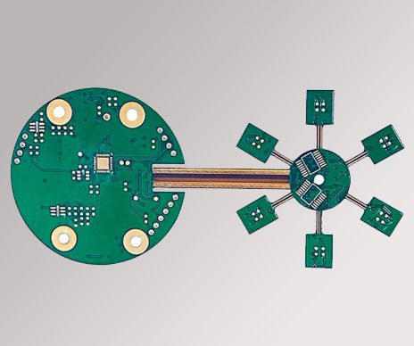
hdi pcb manufacturer
HDI PCB Design
Our design team consists of senior engineers with over 15 years of experience in HDI PCB design. In signal integrity design, we simulate signal transmission scenarios to preempt interference issues. Power integrity analysis ensures stable power supply for each component, while thermal management design addresses circuit board heat problems through strategic layout and material selection. From schematic design to PCB layout, we strictly comply with IPC standards and design for manufacturability principles, validating designs multiple times with advanced software. We’ve assisted numerous clients in optimizing designs, enhancing product performance, and accelerating time-to-market.
HDI PCB Prototyping
Equipped with state-of-the-art equipment, including high-precision laser drillers and electroplating via filling production lines, we offer a rapid 24-hour prototyping service. Every step of the process is closely monitored, from drilling accuracy to electroplating layer thickness, and from circuit pattern clarity to surface treatment quality. Multiple inspection procedures are in place, as we understand that prototype quality is crucial for our clients’ product development.
Mass Production
Our large-scale production base has a monthly capacity of 200,000 square meters. Over the past 20 years, we’ve continuously upgraded our equipment, introduced automated production lines, and adopted advanced manufacturing processes. With certifications such as ISO9001, ISO13485 (medical-grade), and IATF16949 (automotive-grade), we maintain strict quality management. Whether it’s a small order of a few hundred pieces or a large-scale project of tens of thousands of pieces, we guarantee consistent quality and on-time delivery.
HDI PCB Assembly
With more than 10 professional SMT production lines, we can accurately assemble complex components like BGA, CSP, and QFN. Our one-stop services cover component procurement, printing, placement, reflow soldering, and testing. High-end equipment such as X-RAY inspection and AOI optical inspection ensures that every assembled HDI PCB operates stably, providing clients with comprehensive solutions.
Why Choose Us?
Twenty years in the industry have allowed us to amass profound technical expertise and rich practical experience. Our proprietary production processes reduce costs, offering clients cost-effective products. Our comprehensive quality control system, spanning raw material inspection to final product testing, ensures zero-defect HDI PCBs. With our 24/7 customer service, we promptly address any issues clients encounter during design, production, or assembly, ensuring a worry-free experience.
What is the Thinnest PCB Material?
Among PCB materials, Polyimide (PI) film is a popular choice for ultra-thin designs. With a thickness of just a few micrometers, it boasts excellent electrical, mechanical, and high-temperature resistance properties. In HDI PCB manufacturing, PI is often used for thin dielectric layers, enabling the production of extremely thin circuit boards to meet the strict requirements of wearable devices and flexible electronics for lightweight and thin designs.
Advanced HDI Materials for PCB
As HDI technology evolves, so do the materials. Besides Polyimide, Low-Dk materials like BT resin-based materials and specially modified epoxy resins reduce signal transmission losses, enhancing high-frequency signal performance. High thermal conductivity materials, such as ceramic-filled epoxy resins, solve heat dissipation issues in high-power HDI PCB applications. New nanomaterials improve mechanical strength and reliability. We stay at the forefront of material technology trends, constantly exploring new materials to deliver superior HDI PCB products to our clients.
HDI PCB Manufacturing Process
Substrate Preparation
Selecting suitable base materials like FR-4 or Polyimide, we perform surface cleaning and pretreatment. Through processes such as grinding and washing, we ensure a smooth, impurity-free substrate surface, which is essential for subsequent processes and ultimately impacts the final performance of the HDI PCB.
Drilling
Using high-precision laser drillers, we create microvias, buried vias, and through vias according to design specifications, with dimensional accuracy controlled at the micrometer level. Our advanced equipment and skilled technicians guarantee precise drilling, laying the foundation for inter-layer connections and circuit conduction.
Via Metallization
Through electroless copper plating and electroplating processes, we deposit conductive copper layers on the via walls and substrate surfaces, transforming non-conductive via walls into conductive pathways and establishing electrical connections between layers.
Build-up Manufacturing
We coat the substrate with insulating dielectric materials like photosensitive solder masks or liquid photoimageable dielectrics. After exposure and development, new insulating layers and circuit patterns are formed, and copper layers are thickened through electroplating, gradually achieving high-density wiring.
Pattern Electroplating
Electroplating the circuit patterns increases the copper layer thickness, enhancing the conductivity and wear resistance of the circuits, ensuring long-term reliable performance of the circuit boards.
Surface Treatment
Based on product requirements, we choose surface treatment processes such as immersion gold, immersion tin, or OSP (Organic Solderability Preservative). These treatments improve the solderability and oxidation resistance of the circuit boards, extending their service life.
Forming and Testing
We shape the circuit boards through milling and stamping, followed by comprehensive testing, including visual inspection, electrical performance testing (such as continuity and insulation tests), and reliability testing (such as thermal shock and high-temperature, high-humidity tests). Only HDI PCBs that pass all tests are deemed qualified and ready for delivery.
Problems Solved by HDI PCBs
Space Limitation Issues
In small electronic devices like smartphones and wearables, traditional PCBs with low wiring density struggle to accommodate numerous components. HDI PCBs, with their high-density wiring and multi-layer build-up technology, integrate complex circuits in limited spaces, enabling the thin and compact designs that consumers demand.
Signal Transmission Issues
As electronic devices operate at ever-increasing speeds, traditional PCBs can no longer meet signal transmission requirements. HDI PCBs, with their small vias, short transmission paths, and low dielectric constant materials, significantly reduce signal latency, attenuation, and interference, ensuring stable transmission of high-speed signals, which is crucial for applications like 5G communication and high-performance computing.
What is the Difference between HDI and FR-4?
FR-4 is a common general-purpose PCB material, widely used in products with low requirements for wiring density and performance, such as household appliances and low-end consumer electronics. It features low wiring density, large line widths and spaces, mediocre signal transmission performance, and a relatively low cost. In contrast, HDI PCBs, with advanced high-density interconnect technology, have much higher wiring densities, finer line widths and spaces, and superior signal transmission capabilities. However, the complex manufacturing processes result in higher costs, making HDI PCBs the preferred choice for high-end applications where performance and space constraints are stringent, such as smartphones, high-end servers, and medical equipment.
HDI PCB Applications
Consumer Electronics
Widely used in smartphones, tablets, laptops, smartwatches, and wireless earbuds, HDI PCBs enable thin designs and high-performance operation, enhancing user experience.
Automotive Electronics
Applied in automotive engine control units (ECUs), in-vehicle infotainment systems, and autonomous driving assistance systems, HDI PCBs meet the requirements for reliability, stability, and compactness in automotive electronics.
Medical Equipment
In medical devices like CT scanners, MRI machines, and pacemakers, HDI PCBs ensure precise operation and accurate signal transmission with their high-precision wiring and reliability.
Communication Equipment
Used in 5G base stations, routers, and switches, HDI PCBs support high-speed data transmission and signal processing, improving communication network performance.
Aerospace
In satellite communication equipment and aircraft control systems, HDI PCBs, with their high integration, reliability, and ability to withstand harsh environments, meet the strict requirements of the aerospace industry.
Whether you’re in the early stages of product development needing quick prototyping or planning mass production, we offer professional and reliable one-stop HDI PCB solutions. Two decades of dedication and innovation have equipped us with the capabilities to be your trusted partner. Contact us now at sales@pcbtry.com and let’s create leading-edge HDI PCB products together!