


Schematic Diagram PCB Design, PCB Layout
When starting a PCB design, it’s easy to get confused between the schematic diagram and the PCB layout. Both are essential, but they serve very different purposes. In this blog, we’ll break down their roles, explain the PCB design workflow, explore the tools used, and introduce how Thindry circuits, a professional PCB design manufacturer, ensures high-quality outcomes for your projects.
What is a Schematic Diagram?
A schematic diagram is the first and most crucial step in the PCB design process. It’s a logical representation of your circuit using electrical symbols for components like resistors, capacitors, ICs, and connectors. These symbols are linked together with lines representing wires or electrical connections.But here’s the key: a schematic doesn’t care about physical size, shape, or layout. It only focuses on how the components are electrically connected. Think of it like a roadmap showing where each destination (component) connects, but not the exact distance or terrain.
Once completed, this schematic is validated with Electrical Rule Check (ERC) and converted into a netlist—a file that becomes the foundation of your PCB layout.
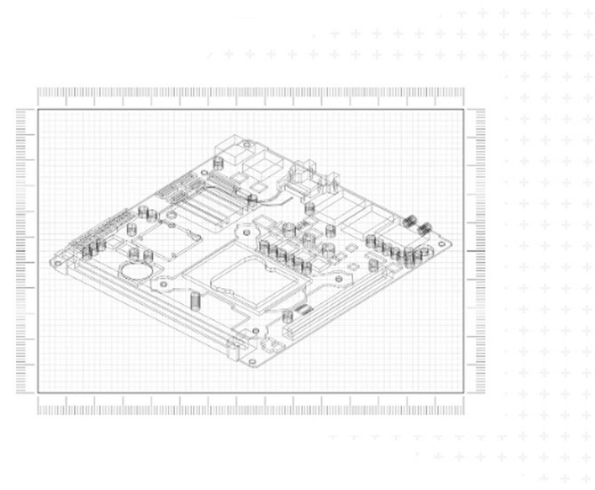
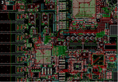
What Does a PCB Layout Do?
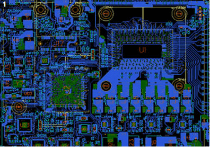
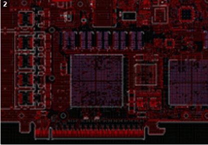
Once the schematic is done, the next step is the PCB layout. This is where the circuit comes to life in a physical format. A PCB layout shows where each component will physically sit on the board and how traces (the copper paths) connect everything.In simple terms, the layout determines:
- The shape and size of your PCB
- Exact placement of all components
- Routing of copper traces between pins
- Power and ground planes
- Vias, pads, silk screen, and solder mask
While the schematic focuses on logic, the layout is all about real-world implementation, including heat management, signal integrity, and manufacturability. That’s why PCB layout is just as important as the circuit design itself.
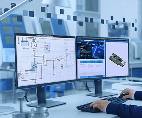
Tools Commonly Used in PCB Design
Both schematic capture and PCB layout require specialized tools. Today’s PCB design software offers integrated environments that handle both parts of the design:- Altium Designer – Widely used for both schematic and layout. Known for its robust features and ease of use.
- KiCAD – Open-source tool popular with hobbyists and startups.
- Cadence Allegro/OrCAD – Ideal for complex, high-speed designs in large enterprises.
- Eagle by Autodesk – Lightweight, beginner-friendly, and good for smaller projects.
Each of these platforms can export Gerber files and drill files—essential documents used by PCB design manufacturers to fabricate and assemble your board.
PCB Design Workflow: From Idea to Real Board
A smooth PCB design workflow helps reduce errors, avoid delays, and cut costs. Here’s a simplified version of what happens from start to finish:- Create the Schematic Diagram
- Design the logical circuit, connect components, and run error checks.
- Generate Netlist
- Convert the schematic into a netlist for use in layout design.
- Start the PCB Layout
- Define the board outline, place components, route traces, and add layers.
- Design Rule Check (DRC)
- Make sure the layout follows electrical and mechanical design rules.
- Export Manufacturing Files
- Generate Gerber, drill, and pick-and-place files.
- Send to PCB Fabrication Team
- Fabrication & Assembly
- Manufacture the bare board and mount components (if needed).
Features and Services of Thindry circuits
As a professional PCB design manufacturer, Thindry circuits provides complete solutions—from schematic capture to final product delivery. We support:
- One-stop PCB design and layout service
- Multilayer board design (up to 40 layers)
- High-speed and RF layout expertise
- Impedance control and signal integrity optimization
- Fast DFM (Design for Manufacturing) review
- Flexible, Rigid-Flex, HDI, and ceramic PCB capabilities
Our team uses industry-standard tools like Altium and Cadence, and we follow IPC standards strictly during every design phase.
How We Make Sure the One-Time Success
When customers come to us for PCB layout and design services, one of their biggest concerns is revision. At Thindry circuits, we aim for one-time success using:- Pre-design review with our engineering team to clarify specs
- Real-time DRC and ERC in design software
- 3D model checking to avoid mechanical collisions
- Design for Manufacturing and Design for Assembly validation
- Prototype fabrication and functional testing before mass production
We understand how important first-pass success is—especially for medical, aerospace, and automotive PCBs. Our strict process helps you avoid costly rework and delays.
Why Thindry circuits Is Globally Recognized
With global customers across North America, Europe, and Asia, Thindry circuits has become a trusted PCB design manufacturer for industries that demand precision and performance. Here’s why customers choose us:- Use of MES system to trace every component and design step
- Competitive pricing and fast lead time
- Professional English-speaking support team
- Over 18 years of experience serving OEMs and ODMs
Whether you need a complex high-frequency PCB or a reliable consumer electronics board, our team delivers both design and manufacturing under one roof.
A successful PCB design starts with a clear schematic and ends with a well-executed layout. While the schematic defines the logic, the layout translates it into a physical reality. Working with an experienced PCB design manufacturer like Thindry circuits ensures your concept becomes a reliable product—with no surprises during production.
From start to finish, our design and layout services help engineers bring innovation to life faster and smarter.
Frequently Asked Questions (FAQs) 1. Can I design a PCB without making a schematic?It's possible but not recommended. The schematic ensures the logic is correct, which is critical for complex designs.
2. What's the difference between PCB design and PCB layout?
PCB design refers to the whole process (schematic + layout), while PCB layout focuses only on the physical design part.
3. Which software is best for beginners in PCB design?
Eagle and KiCAD are great for beginners due to their simplicity and community support.
4. How much does PCB layout service cost?
Costs vary depending on board complexity, layers, and turnaround time. Contact Thindry circuits for a fast quote.
5. Can Thindry circuits help with component sourcing?
Yes. We offer BOM validation, sourcing, and even full turnkey PCB assembly.