
A heavy copper PCB is a printed circuit board built with thicker copper than a standard board, designed to carry higher current, improve heat dissipation, and deliver better durability in demanding applications. It is widely used in power electronics, automotive systems, industrial equipment, renewable energy, and high-reliability products.
If you are evaluating a heavy copper PCB, the most important questions are not only how thick the copper is, but also how the board will handle current, temperature rise, solderability, layer balance, and long-term reliability. The right specification depends on electrical load, thermal stress, board structure, and manufacturing capability.
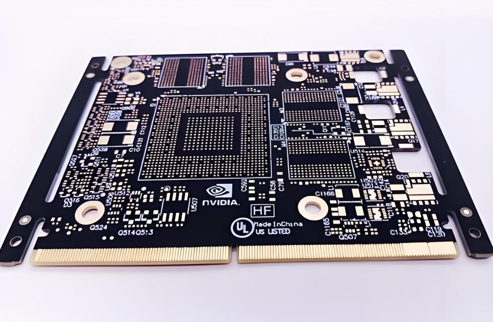
Heavy Copper PCB
What Is a Heavy Copper PCB?
A heavy copper PCB is a circuit board with copper thickness significantly greater than that of standard FR-4 boards. While common copper weights are 0.5 oz to 2 oz, heavy copper PCBs typically start around 3 oz and can go much higher depending on the design.
These boards are used when standard copper cannot safely carry the required current or dissipate enough heat. The thicker copper also improves mechanical strength and can increase the board’s tolerance to thermal cycling and power surges.
Why Heavy Copper PCB Design Matters
Heavy copper PCB design matters because power density is increasing across modern electronics. Devices are running at higher current, smaller size, and stricter thermal limits, which means the PCB itself must act as part of the power and thermal management system.
In many projects, using a heavy copper PCB can reduce voltage drop, improve reliability, and lower the risk of overheated traces, pad lifting, and premature failure.
How Does a Heavy Copper PCB Work?
A heavy copper PCB works by increasing the cross-sectional area of copper conductors. A larger copper cross-section reduces electrical resistance, which helps lower heat generation under load.
Because copper also spreads heat laterally, thicker copper layers help distribute thermal energy away from hotspots. This is especially useful in power conversion, charging, and motor drive circuits.
Common Types of Heavy Copper PCB
Heavy copper PCBs are available in several structures, each suited to a different technical requirement. The board type should match current load, thermal profile, and assembly complexity.
| Type | Typical Use | Key Benefit | Limitation |
|---|---|---|---|
| Single-layer heavy copper PCB | Power modules, simple power distribution | High current capacity, simple structure | Limited circuit complexity |
| Multilayer heavy copper PCB | Industrial control, automotive electronics | Combines power handling with signal routing | Higher manufacturing difficulty |
| Heavy copper flex-rigid board | Compact systems with moving parts | Flexibility plus current handling | More expensive and harder to fabricate |
| Metal-core power board | LED, power modules, thermal applications | Strong heat dissipation | Less suitable for dense multilayer routing |
What Materials Are Used in Heavy Copper PCB Manufacturing?
Heavy copper PCBs are usually built on FR-4 substrates, although high-Tg materials, polyimide, metal-core structures, and other special laminates may be used for higher thermal or electrical performance.
The copper foil, prepreg system, solder mask, surface finish, and laminate resin must all be selected carefully. If the copper is very thick, the board may require special drilling, etching, plating, and lamination controls to maintain dimensional accuracy and hole quality.
How Heavy Copper PCBs Are Manufactured
Manufacturing a heavy copper PCB is more demanding than making a standard board because thick copper is harder to etch, plate, and control uniformly. The process usually requires tighter process windows and more inspection points.
Common challenges include under-etching, over-etching, uneven plating thickness, resin recession, poor hole wall coverage, and layer imbalance. A capable manufacturer must control these risks with stable process capability and in-house testing.
Key Manufacturing Challenges and Failure Risks
Heavy copper PCB failure often starts with process variation. If the copper thickness is not uniform or the hole plating is insufficient, the board may fail under high current or thermal stress.
Typical failure modes include trace cracking, pad separation, delamination, via barrel cracks, solder mask lifting, and local overheating. In field use, these problems are often triggered by poor thermal design, overload, vibration, or repeated power cycling.
How to Test a Heavy Copper PCB
Testing a heavy copper PCB should cover both electrical and physical reliability. Standard checks usually include continuity testing, insulation resistance testing, solderability inspection, cross-section analysis, and dimensional verification.
For power applications, additional thermal imaging, current load testing, and vibration testing may be necessary. In high-reliability projects, IPC-related workmanship requirements and application-specific standards should be referenced during acceptance.
Heavy Copper PCB vs Standard PCB
The main difference between a heavy copper PCB and a standard PCB is current capacity, heat handling, and mechanical robustness. Standard PCBs are suitable for general signal routing, while heavy copper boards are better for power-intensive designs.
| Parameter | Standard PCB | Heavy Copper PCB |
|---|---|---|
| Copper thickness | Typical 0.5 oz to 2 oz | Usually 3 oz and above |
| Current handling | Moderate | High |
| Heat dissipation | Standard | Better thermal spreading |
| Manufacturing difficulty | Lower | Higher |
| Cost | Lower | Higher |
Where Heavy Copper PCBs Are Used
Heavy copper PCBs are used in industries where power, heat, and reliability are critical. They are especially common in automotive electronics, renewable energy systems, industrial power supplies, battery management systems, motor drives, charging systems, and LED power modules.
They are also used in aerospace, medical devices, and advanced industrial systems where failure tolerance is low and thermal performance is important.
Heavy Copper PCB Design Considerations
Designing a heavy copper PCB requires attention to trace width, current load, thermal relief, via design, layer stack-up, and assembly compatibility. The copper weight must be matched to actual operating conditions rather than chosen only for safety margin.
Designers should also consider component spacing, soldering temperature profile, hole size, and copper balance across layers. Poor planning can cause assembly defects or unreliable field performance even if the board passes initial testing.
How to Choose the Right Heavy Copper PCB
The right heavy copper PCB depends on current, voltage, temperature rise, board size, and cost target. If the application involves sustained high current or repeated surge loading, thicker copper and stronger thermal management are usually necessary.
For complex products, it is often better to ask the manufacturer for stack-up advice, thermal analysis, and manufacturability feedback before finalizing the design. That helps avoid costly redesigns later.
Cost Factors in Heavy Copper PCB Production
Heavy copper PCB cost is influenced by copper thickness, layer count, board size, material selection, drilling difficulty, plating requirements, and testing level. The thicker the copper and the more complex the structure, the higher the manufacturing cost.
Yield also affects cost. If the design creates low manufacturability or high scrap risk, the total project cost may rise significantly even if the unit price looks acceptable at first glance.
Supply and Quality Control for Heavy Copper PCB Orders
A reliable supplier should be able to provide stable process control, inspection reports, and engineering support. For bulk production, quality consistency matters more than sample performance alone.
Before placing an order, buyers should confirm copper thickness tolerance, hole plating quality, surface finish, lamination capability, test methods, delivery time, and change-control process. For China source factories, the advantage is direct engineering communication and scalable production support.
Heavy Copper PCB Applications in Different Industries
Heavy copper PCB applications are expanding as electronics become more power-dense. In automotive systems, they support power distribution and battery control. In industrial equipment, they improve reliability under continuous load. In energy systems, they help stabilize high-current paths and reduce heat concentration.
In LED and power electronics, they are used to extend service life and manage thermal stress. In all these cases, the board is not just a carrier of circuits — it is part of the thermal and electrical solution.
Frequently Asked Questions
What copper thickness is considered heavy copper PCB?
A board is generally considered a heavy copper PCB when the copper thickness exceeds standard values, often starting at 3 oz and above. The exact threshold can vary by industry and manufacturer.
Is a heavy copper PCB always better than a standard PCB?
Not always. Heavy copper improves current carrying and heat handling, but it also increases cost, weight, and manufacturing complexity. It should be selected only when the application truly needs it.
Can heavy copper PCBs be multilayer boards?
Yes. Heavy copper PCBs can be made in multilayer structures, but the process is more difficult. The manufacturer must control plating, lamination, and hole quality carefully.
What are the main failure risks in heavy copper PCB design?
The main risks are poor thermal design, trace cracking, via failure, delamination, and inconsistent plating thickness. These issues usually come from either design mistakes or process instability.
How do I know if my project needs a heavy copper PCB?
If your circuit carries high current, generates significant heat, or must operate reliably under power stress, a heavy copper PCB may be appropriate. A thermal and electrical review is recommended before final selection.
Are heavy copper PCBs suitable for automotive electronics?
Yes. They are commonly used in automotive power modules, battery systems, charging equipment, and control units where durability and current capacity are important.
What is the biggest challenge in manufacturing heavy copper PCB?
The biggest challenge is process control. Thick copper is harder to etch, plate, and inspect consistently, so the manufacturer must maintain tight control over all critical steps.
Can heavy copper PCB reduce overheating?
Yes. Thick copper helps spread heat more effectively and reduces conductor resistance, which can lower temperature rise in power circuits.
Is heavy copper PCB expensive?
Compared with standard PCB, yes, it is usually more expensive because of the extra material, process complexity, and quality control requirements. The added cost is often justified in high-power applications.
What should I check before ordering heavy copper PCB?
Check copper weight, stack-up, hole plating, surface finish, test method, manufacturing tolerance, and the supplier’s experience with power boards. Engineering review before production can reduce risk.
Can heavy copper PCB be repaired if damaged?
Minor defects can sometimes be repaired, but severe trace damage, delamination, or via failure may make replacement safer than repair. Reliability should be the first consideration.
What industries benefit most from heavy copper PCB?
Industries with high current and thermal stress benefit most, including automotive, renewable energy, industrial control, LED power, and battery systems.
Conclusion
A heavy copper PCB is a practical solution for high-current and high-heat electronics, but the best results come from matching copper thickness, stack-up, thermal design, and manufacturing capability to the real application. Choosing the wrong structure can increase cost without improving reliability.
For engineers and buyers, the smartest approach is to evaluate electrical load, thermal behavior, and supplier process control together. A reliable source factory can help optimize the design, improve manufacturability, and reduce hidden failure risks before mass production.
If you’re sourcing reliable PCB/PCBA manufacturing — OEM, ODM, prototyping, mass production, or custom engineering solutions — reach out to our engineering team for technical support and a quote at sales@pcbtry.com. If you are looking for keywords-related products or services, please contact us at sales@pcbtry.com.


0 Comments