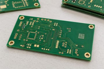
Blog
PCB Laser Marking Materials: Mask, Laminate and Validation
Learn which PCB surfaces can be laser marked and how to validate samples, code readability and board integrity before approving a production marking process.




Learn which PCB surfaces can be laser marked and how to validate samples, code readability and board integrity before approving a production marking process.
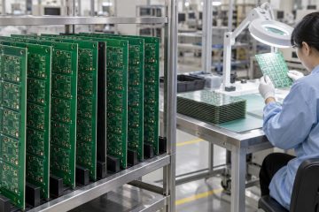
Learn how to optimize bare PCB production using first-pass yield, defect data, bottleneck checks and controlled trials without weakening acceptance requirements.
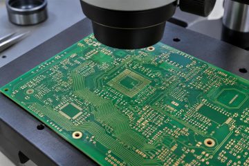
Compare semi-additive PCB processing and subtractive etching, then review line geometry, copper thickness, via rules and qualification before layout release.
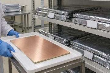
Control PCB laminate and prepreg from receiving to layup with product-specific storage checks, cut-sheet traceability and practical material-release decisions.
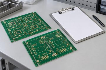
Use a PCB manufacturing process audit checklist to trace a real job, review process records, document findings and verify corrective-action closure.
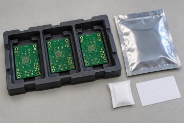
Plan a PCB packaging process with separate ESD, moisture and mechanical controls, plus sealing, labeling and receiving checks for board shipments.
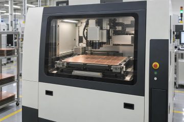
Follow the PCB laser drilling process from stackup review to microvia inspection, with target-pad, cleaning and plating checks for an HDI build.
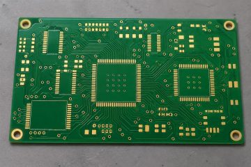
Understand the PCB ENEPIG process, each metal layer’s role, and the inspection records needed to approve soldering or wire-bond applications.
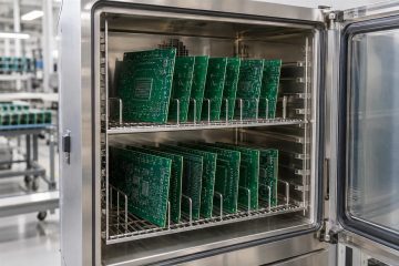
Learn when bare PCBs need baking, how to approve temperature and time, and what to record before releasing boards to assembly or dry storage.
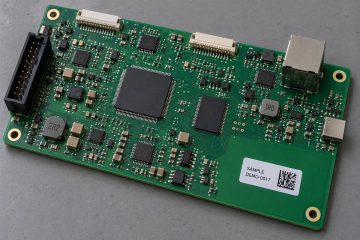
Plan a PCB labeling process with controlled serial numbers, suitable label materials, placement rules, scan checks and records that survive production.
If you have any enquiry about quotation or cooperation, please feel free to email us at sales@pcbtry.com or use the following enquiry form. Oursales representative will contact you within 24 hours. Thank you for your interest in our products.