




What the Nickel-Palladium-Gold Stack Does
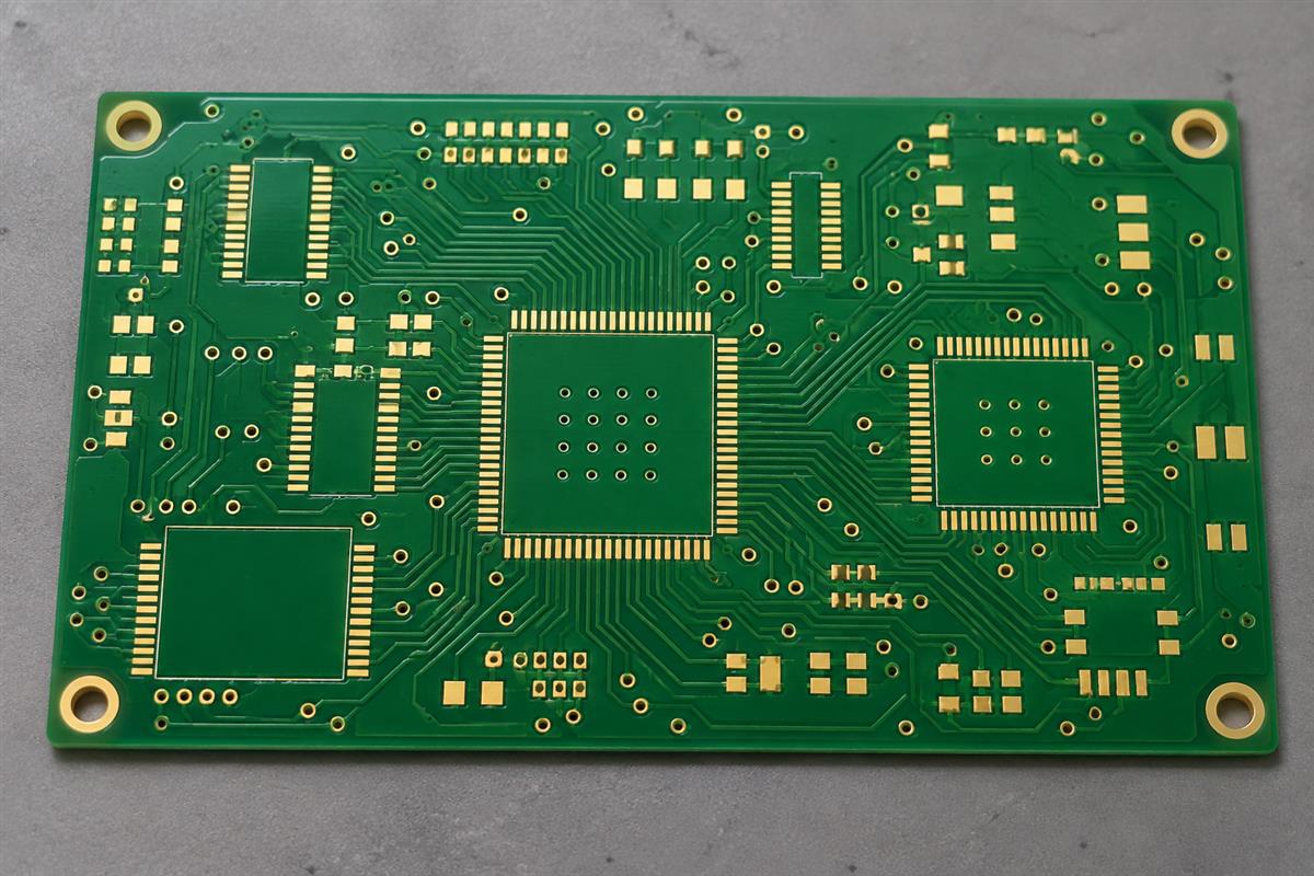
The PCB ENEPIG process deposits electroless nickel, electroless palladium and immersion gold onto exposed copper features. Think of it as a thin, three-metal interface between the copper circuit and the connection you will make during assembly. It is a surface finish, not the process that builds the copper tracks or plates a through-hole.
The practical question is not simply whether a board has ENEPIG. It is whether that particular finish, on that pad geometry, will support your soldering or wire-bonding process. A gold-colored pad does not identify the coating stack, prove its thickness or establish bond reliability.
| Layer | Its practical role | What you still need to verify |
|---|---|---|
| Nickel over copper | Provides a barrier between copper and the outer finish and establishes the underlying interface. | Deposit condition, specified thickness and the chemistry or composition required by the qualified process. |
| Palladium over nickel | Separates nickel from the gold deposition environment and contributes to the solderable or bondable finish system. | Coverage, thickness and the approved palladium process. Pure palladium and palladium-phosphorus offerings are not automatically interchangeable. |
| Gold at the surface | Provides a protective, assembly-facing surface over the palladium. | Coverage, surface cleanliness and compatibility with the intended assembly operation. |
ENIG omits the palladium layer. EPIG omits nickel. Those differences matter: substituting one finish name for another changes the stack, even if the boards look similar. ENEPIG also should not be specified as a direct replacement for wear-resistant hard gold on repeatedly mated edge contacts.
Atotech’s final-finishing portfolio describes several palladium and gold chemistries. This is why an approved process designation is more useful than a purchase order that only says “gold finish.” Do not assume every commercial ENEPIG line uses identical deposition reactions.
The ENEPIG Process from Copper Preparation to Final Rinse
The process follows the metal stack: prepare exposed copper, establish an active surface, deposit nickel, deposit palladium, apply gold, then rinse and dry. Intermediate rinses and checks belong to the qualified line sequence too. This is an explanation for engineering and purchasing decisions, not a chemical-bath recipe: concentrations, dwell times, temperatures and replenishment limits must come from the approved chemistry supplier and manufacturing process.
1. Prepare the exposed copper
The input is a fabricated board with defined areas that require finish. Cleaning and controlled surface preparation remove conditions that would interfere with deposition. The manufacturer must control preparation without damaging the fine copper features or adjacent solder mask. Incomplete cleaning can leave local skip plating; excessive preparation can change feature geometry. Review the incoming condition, process records and inspection findings rather than assuming later gold will hide a preparation defect.
2. Activate the surface for nickel deposition
The prepared copper must initiate deposition uniformly in the selected process. Activation chemistry and the preceding rinse condition therefore matter. The purpose is consistent initiation, not a visible decorative coating. Poor initiation may appear later as incomplete coverage. Evidence should connect the approved pretreatment sequence to coverage checks on representative features. Technic’s final-finish process descriptions illustrate the relationship between copper activation, electroless nickel, palladium and gold; their proprietary settings are not universal instructions.
3. Deposit the electroless nickel layer
Nickel is deposited onto the activated features. The line must control both the deposit and the bath condition, using its approved operating window. A thickness reading alone does not describe every property of the nickel layer. When nickel-phosphorus chemistry is used, the specified composition and process qualification may also matter. Nonuniform or damaged underlying deposits can compromise the interfaces above them. The release evidence should identify the process, lot and nickel measurements, with escalation for abnormal surface condition.
4. Deposit the electroless palladium layer
Palladium is applied over nickel before gold. Its continuity and controlled deposition are important to the intended layer separation. Check that the actual palladium chemistry matches the qualified finish rather than accepting a substitution solely because both products contain palladium. A missing or inadequately covered area cannot be ruled out by a distant measurement on a large pad. Pair the line records with a measurement and inspection plan appropriate to the board’s critical features.
5. Apply the gold finish
Gold is applied over the palladium using the specified finishing process. The traditional ENEPIG name refers to immersion gold, while commercial systems may incorporate different reaction mechanisms. Gold deposition must remain inside the approved process window; a longer exposure is not automatically a better finish. Check the gold result and investigate abnormal interfaces or corrosion indications through the qualified failure-analysis route. The presence of palladium is not a blanket guarantee against every plating defect.
6. Complete rinsing, drying and controlled handling
The coated board needs appropriate final rinsing, drying, inspection and packaging. Residues or handling contamination can undermine an otherwise acceptable deposit. Do not touch connection surfaces merely because they look robust. Record the finish lot, inspection disposition, packaging conditions and applicable storage requirements. If the board is reworked or chemically cleaned later, review compatibility before treating the original finish approval as unchanged.
Each stage depends on the previous one. Finding a final defect should trigger a traceable investigation through preparation, bath control and handling, not an automatic instruction to add more gold.
Specify the Finish for Soldering, Wire Bonding or Both
Choose the acceptance plan from the connection you need to make. ENEPIG is used in soldering and wire-bonding applications, but approving one operation does not qualify every other operation on the same board. Wire material, bonding method, pad geometry and prior thermal exposure all belong in the discussion.
| Intended use | Information to provide | Evidence to agree before production |
|---|---|---|
| Soldered components | Assembly sequence, solder system, expected thermal exposures and critical pad types. | Applicable solderability requirements and an assembly validation plan with defined acceptance criteria. |
| Wire-bond pads | Wire material and diameter, bonding method, pad dimensions and relevant process history. | Bond-process qualification, appropriate pull or shear testing, and acceptable failure-mode criteria. |
| Mixed solder and wire-bond assembly | Which areas serve each function and the order of reflow, cleaning and bonding. | Validation representing the actual sequence, including the condition of bond pads after earlier operations. |
| Repeatedly mated contact surfaces | Contact mechanics, mating-cycle requirements and electrical environment. | A separately justified contact-finish specification; do not approve ENEPIG merely because its surface is gold. |
For example, suppose components are reflowed before wire bonding. A successful bond trial on a fresh, unheated coupon does not by itself validate the later production sequence. A representative trial must address the prior thermal and cleaning history. Define that sequence with the PCB assembly team before releasing the bare-board finish.
MacDermid Alpha’s ENEPIG product information describes soldering and wire-bond applications for its process. That supplier-specific capability is a starting point for qualification, not evidence that an unidentified production lot meets your assembly requirements.
Verify Thickness, Surface Condition and Assembly Performance
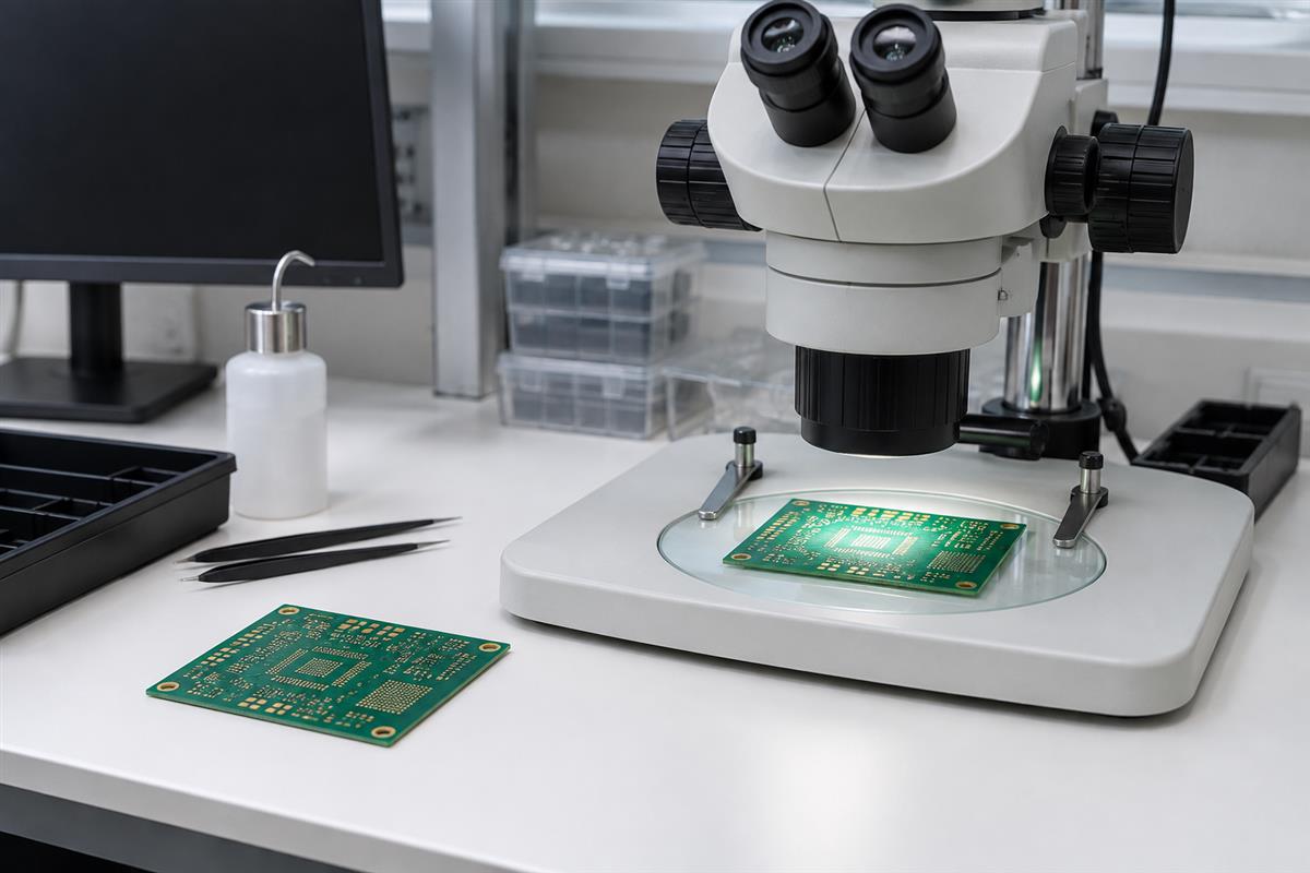
Use three separate questions: are the specified layers present at acceptable thickness, is the surface and interface condition acceptable, and does the assembly connection meet its own requirements? No single photograph or test report answers all three.
| Evidence | Useful conclusion | What it does not establish alone |
|---|---|---|
| Qualified multilayer XRF measurement | Thickness or composition results within the instrument method’s scope at measured locations. | Every pad’s condition, absence of all interface defects, or acceptable bond strength. |
| Visual or microscopic inspection | Visible coverage issues, contamination or other observable anomalies within the inspection capability. | Identity and thickness of ultrathin buried layers. |
| Targeted cross-section or failure analysis | Additional evidence about the sampled structure or investigated failure. | Automatic representation of every location in the lot. |
| Solderability or assembly testing | Performance under the specified test or assembly conditions. | Qualification of a different thermal profile, storage history or bonding process. |
| Wire-bond pull or shear evaluation | Connection performance and failure behavior under an agreed method. | Universal suitability for other wire materials or bonding settings. |
X-ray fluorescence, or XRF, can be used for nondestructive coating measurements with a suitable instrument and method. For ENEPIG, ask whether the setup is qualified for the actual multilayer stack, pad dimensions and expected thickness range. Spot size, calibration, substrate model and measurement uncertainty affect how a result should be interpreted. An ordinary caliper cannot resolve these coating layers. Fischer’s electronics measurement guidance specifically addresses ENIG and ENEPIG applications; its coating-measurement overview explains the role of XRF for metallic coatings.
A simple reporting example: 0.10 micrometers equals 100 nanometers. These are the same thickness expressed in different units, not two different results. This is a unit-conversion example, not an ENEPIG acceptance limit. If a reported result lies close to a drawing limit, request the measurement uncertainty and agreed acceptance decision rule rather than rounding the value until it passes.
Also ask where measurements were taken. A convenient large coupon may not address the smallest critical bond pads without evidence that it represents their finish. The inspection plan should state locations, sampling, individual results and how nonconforming findings are handled. These details make a quality-control record useful for release decisions instead of merely documenting that inspection occurred.
IPC-4556 identifies the specification for electroless nickel/electroless palladium/immersion gold plating for printed boards. State the agreed edition and any customer additions in the purchase documents. Obtain the applicable standard for its detailed requirements; an internet summary is not a substitute for the contractual specification.
What to Put in an ENEPIG RFQ and Release Record
An effective ENEPIG request tells the fabricator what must work and what proof you need. Send the board data with a finish note tied to the drawing revision, then resolve missing acceptance criteria before production.
- Define the finished areas: identify solder pads, bond pads and any other exposed features; include relevant dimensions.
- Name the required finish: specify ENEPIG and the agreed standard edition, drawing requirements and any qualified process restrictions.
- Explain the assembly sequence: provide soldering, cleaning and bonding operations that could affect the surfaces.
- Agree the measurement plan: state layer requirements, measurement locations, representative coupons, sampling and the handling of uncertainty.
- Agree performance validation: identify required solderability or bond tests, test conditions, criteria and responsibility for approval.
- Define traceability and handling: request lot-linked records and the applicable packaging, storage and subsequent handling instructions.
- Control changes: require review of finish substitutions, process changes or rework that could invalidate the approved basis.
Before release, check that the certificate and reports match the correct board revision and lot. Missing test conditions are not fixed by a certificate that simply says “pass.” Resolve discrepancies with the responsible quality or engineering team and document the disposition.
To discuss a board requiring ENEPIG, contact PCBtry with the fabrication data, finish specification, critical pad details, quantity and assembly sequence. Ask for confirmation of finish availability, process compatibility and the evidence that can be supplied before approving the order.
FAQ
Can I identify ENEPIG by its gold color?
No. Similar-looking gold surfaces can have different underlying layers. Use traceable manufacturing records and suitable verification, not color, to identify the specified finish.
Is ENEPIG the same as hard gold?
No. A finish intended for soldering or bonding is not automatically qualified for repeated sliding contact. A wear-contact application needs its own finish and performance requirements.
Does ENEPIG eliminate every nickel corrosion risk?
No. Palladium changes the interface and deposition environment, but process control and inspection still matter. Investigate suspicious results rather than treating the finish name as a defect-free guarantee.
Can a nickel-free application use ENEPIG?
Not as a nickel-free stack: nickel is part of ENEPIG. Discuss a different finish system and qualify it for the intended application instead of silently deleting a layer.
Can one thickness reading release the whole lot?
Only if it satisfies the agreed sampling and release plan, which must be appropriate to the risk. One convenient reading should not be assumed to represent all critical features without a justified plan.
Does more gold always improve the result?
No. The finish must meet the specified window and assembly requirements. Changing deposition exposure or thickness without qualification can change the process result rather than simply improve it.
Can a passed solder test approve wire bonding?
No. Soldering and wire bonding form different connections. Wire bonding needs evaluation of its own material, method, thermal history and acceptance criteria.
What should I do if a report has no units or test conditions?
Request a corrected, traceable report before using it for release. Confirm the measured layer, units, locations, method, acceptance criteria and applicable decision rule.



0 Comments