




What Laser Drilling Must Achieve in an HDI Board
The PCB laser drilling process removes material with controlled laser pulses to form small holes, commonly blind microvias in high-density interconnect boards. For a blind microvia, the goal is to open the dielectric down to a specified copper target pad without damaging that pad, then leave a surface suitable for the subsequent cleaning and metallization process.
Think of the target pad as the copper landing surface at the bottom of a shallow well. Drilling creates access to it. Later copper deposition creates the conductive connection. A round opening on the surface is therefore only an intermediate result, not proof of a reliable interconnect.
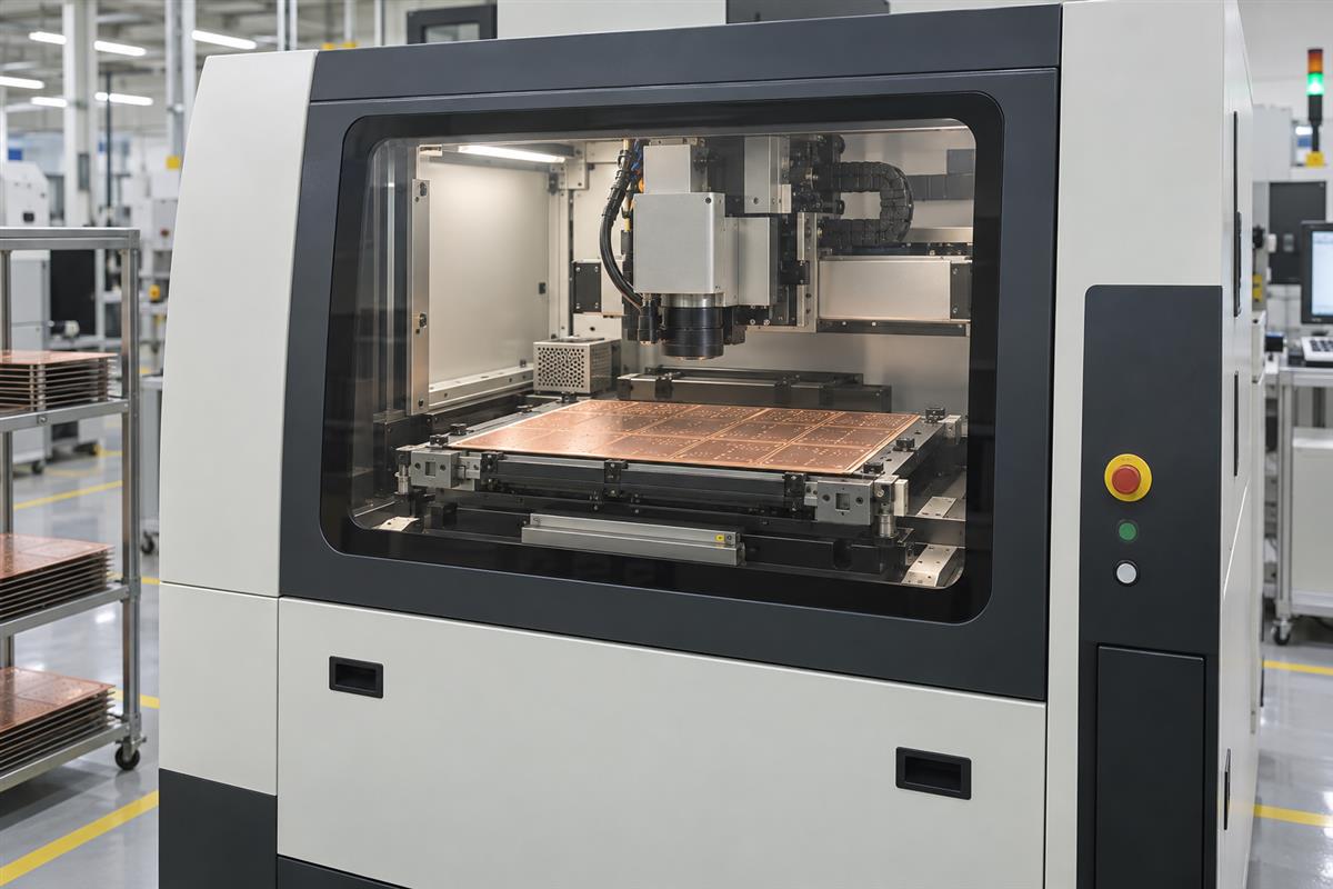
This guide focuses on production laser microvias. It is different from engraving a circuit pattern on copper or drilling mounting holes with a rotating bit. For the wider process context, see the PCB drilling overview.
Three questions should drive the review: did the hole reach the intended target, is that target in an acceptable condition for plating, and does the completed connection survive the specified manufacturing and service stresses? The answers require different evidence.
The PCB Laser Drilling Process from Data Review to Plating Handoff
A controlled process links the released stackup and hole data to panel alignment, material removal, post-drill cleaning and a documented plating handoff. Exact laser and chemical settings are qualified for the machine, materials and geometry; there is no safe universal power-and-pulse recipe.
1. Define the layer connection and material stack
Engineering starts with the stackup, drill data, copper artwork and required via structure. Confirm the start and target layers, dielectric thickness, entry geometry and target-pad dimensions. Distinguish the drilled opening from the required finished plated structure. A wrong layer span can produce a neatly formed hole that connects the wrong part of the circuit. Resolve drawing conflicts before machine programming and retain the approved layer-pair definition.
2. Establish the surface and laser-processing route
The incoming copper and dielectric condition must suit the chosen route. Some processes use an opening in the outer copper; others use an appropriate direct-drilling preparation or a laser sequence able to process both copper and dielectric. Control material identity and surface preparation because a recipe that works on one build may not transfer to another. The evidence should identify the qualified material/route combination and the first-piece requirements, not simply the machine model.
3. Register the panel and verify the setup
The machine must align the drilling pattern with the real panel, not only with nominal CAD coordinates. Fiducial recognition and relevant dimensional compensation address the relationship between artwork and processed features. Fixture support and setup consistency also matter. Misregistration can reduce the available target-pad landing area even if hole diameter is correct. Verify representative locations and retain the registration and first-piece results before releasing the lot.
4. Ablate the opening while protecting the target pad
The qualified pulse sequence removes the required material. Insufficient removal may leave residue at the bottom; excessive processing can damage the target copper or surrounding material. The operator controls the approved process window rather than increasing energy until the hole looks open. Check the relevant geometry and target condition at the defined sampling points. Stop and investigate abnormal results before repeating them across a panel.
LPKF’s UV microvia description explains processing through copper and dielectric with controlled energy. Its product-specific performance statements are not universal acceptance criteria for all PCB materials.
5. Remove debris and qualify the surface for metallization
The drilled opening enters the approved post-laser cleaning route. Surface spatter, dielectric residue and the condition of exposed copper are separate issues; one cleaning operation should not be assumed to solve all of them. Inadequate preparation can leave a poor interface for later metal deposition, while excessive treatment can change geometry or attack material. Review the cleaned feature and the process records against the agreed criteria before releasing it to plating.
Atotech’s integrated interconnect sequence treats laser preparation, spatter removal, desmear and metallization as connected operations. The practical lesson is to qualify their interaction, not just the drilling step in isolation.
6. Transfer to metallization, filling and final verification
A clean hole is still not a plated connection. Transfer the panel with its identity and inspection disposition to the specified metallization and, where required, via-filling route. A later defect must be traceable to the relevant drilling, cleaning and plating history. Retain the lot linkage and verify the completed structure with the required dimensional, electrical and reliability checks. Otherwise, a drilling approval can be mistaken for approval of an unfinished interconnect.
Industrial laser processing requires suitable enclosed equipment, extraction and trained operation under the equipment manufacturer’s safety procedures. Do not attempt to reproduce an HDI drilling process with an open hobby engraver or bypass an interlock.
Choose the Laser Route Around the Actual Material Stack
Choose the route from the materials and target geometry, not from a claim that UV or CO2 is always better. Absorption, copper preparation, dielectric composition and the required stop condition affect the workable process.
| Route or condition | What to confirm | What not to assume |
|---|---|---|
| UV process through copper and dielectric | Qualified material stack, copper thickness and target-pad protection. | One published equipment capability covers every material and hole size. |
| CO2-based route | How the entry copper is prepared or opened and how the dielectric is processed. | The route is identical to UV processing or never needs surface preparation. |
| Mixed or staged process | Which operation opens copper, removes dielectric and conditions the target. | A single machine description explains the whole manufacturing sequence. |
| New resin, reinforcement or copper construction | Whether the existing drilling and cleaning qualification still applies. | A familiar board thickness makes the old recipe transferable. |
Atotech describes CO2-compatible surface preparation as part of its integrated offering. LPKF describes UV systems that process copper and substrate together. These examples show why an RFQ should ask for the proposed manufacturing route rather than dictate a generic wavelength.
For setup evidence, LPKF’s MicroLine documentation describes vision-based alignment and laser-power measurement at material level. Those are examples of controlled variables. A supplier still needs to show that its own equipment and process are qualified for your construction.
Inspect the Hole, Then Validate the Finished Interconnect
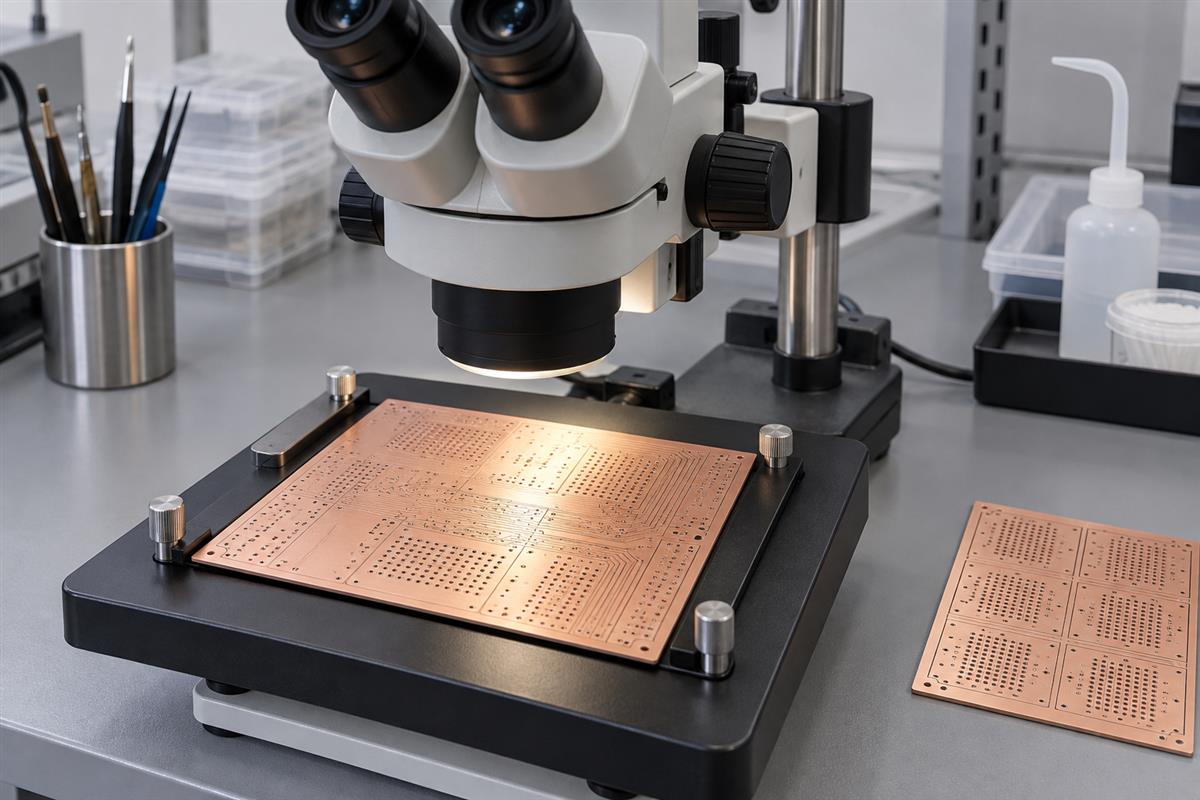
Inspection must progress from the drilled geometry to the cleaned interface and finally the plated connection. A surface photograph, a microsection and an electrical test each answer different questions.
| Stage and evidence | Useful finding | Limit to remember |
|---|---|---|
| Top-view optical inspection after drilling | Location, entry appearance and visible abnormalities at sampled features. | Does not by itself prove every buried interface is clean or undamaged. |
| Cleaned-hole inspection or targeted analysis | Evidence relevant to residual material and target condition. | Method sensitivity and sampling must match the defect being investigated. |
| Microsection of the completed via | Sampled geometry, copper coverage and visible structural features. | A section is local evidence, not a guarantee against every latent interface failure. |
| Electrical continuity and isolation testing | Electrical behavior under the stated test conditions. | Room-temperature passage alone does not establish thermal-stress reliability. |
| Agreed performance or reliability testing | Response of representative structures to specified exposures. | The test must represent the actual construction and acceptance requirements. |
Geometry example: suppose a proposed microvia has a 60 micrometer dielectric depth and an 80 micrometer entry diameter. Depth divided by that diameter is 0.75. This arithmetic example is not an acceptance limit. If a drawing or supplier uses a different diameter definition, the comparison changes. Record the top opening, bottom geometry and depth explicitly, then ask the fabricator to confirm manufacturability and the applicable criteria.
The reason for separating tests is not theoretical. In its 2019 microvia reliability warning, IPC described latent interface failures that escaped traditional acceptance and appeared later. Treat that historical warning as a reason to agree appropriate performance evidence, not as a current specification table or proof that every stacked microvia will fail.
Likewise, a clean-looking target is not permission to skip the qualified metallization sequence. Atotech’s desmear and metallization guidance addresses coverage in challenging blind-via geometries. The completed interface depends on more than visible hole shape.
What an HDI Laser-Drilling RFQ Must Define
A useful RFQ defines the desired connection and its acceptance evidence. “Smallest laser hole” is not enough to determine whether the complete build is feasible or reliable.
| Send or specify | Why it changes the review | Ask the supplier to return |
|---|---|---|
| Released fabrication data and stackup | Establishes layers, materials and target locations. | Confirmed build sequence and unresolved data questions. |
| Via layer pairs and geometry | Defines depth, landing area and the required finished structure. | Manufacturability comments with any proposed dimensional changes. |
| Stacked, staggered or other arrangement | Changes the construction and qualification discussion. | Proposed fabrication and validation basis for that arrangement. |
| Fill, cap and assembly requirements | Connects drilling to plating and component attachment. | Clear scope and handoff conditions. |
| Acceptance specification, edition and customer additions | Prevents an undefined “IPC compliant” approval. | Agreed inspection, coupons, sampling and reports. |
Before authorizing production, check that:
- The proposed layer connection matches the design revision.
- Material substitutions and process changes have defined approval rules.
- The inspection plan distinguishes drilling, cleaning and finished-via checks.
- Any required reliability test represents the intended microvia construction.
- Reports can be traced to the production lot and approved drawing.
- Nonconforming findings have a documented disposition before shipment.
For a board using laser microvias, review PCBtry’s HDI PCB service and send the fabrication package for review. Include the stackup, via layer pairs, geometry, quantities and inspection requirements. Ask for confirmation of the proposed process and evidence before approving the build.
FAQ
Does laser drilling make a hole conductive?
No. It forms the opening. The specified metallization and plating operations create the conductive path; their results must be verified separately.
Is every laser-drilled hole a blind microvia?
No. Laser equipment can perform several kinds of material removal. The start layer, end layer, geometry and intended function define the feature in your drawing.
Can I use the same settings for every FR-4 board?
No. Material construction, copper, dielectric depth and the qualified cleaning route can differ. Use settings validated for the actual build.
Does a copper target pad stop all lasers automatically?
No. Material interaction and process settings determine what is removed or damaged. Protecting the target requires a qualified process, not reliance on the word “copper.”
Can a hole look clean and still have an interface problem?
Yes. Visual appearance alone may not resolve every residue or interface issue. Select an inspection or analysis method appropriate to the suspected problem.
Is a 0.75 aspect ratio always acceptable?
No. The example above is arithmetic only. Manufacturability and acceptance depend on the geometry definition, materials, processing and specified requirements.
Does passing continuity prove long-term microvia reliability?
No. It establishes behavior at the test conditions. Agree additional performance testing when the construction and application require it.
What should change when the dielectric material changes?
Review drilling, cleaning, plating compatibility and the validation basis. Do not transfer approval only because the replacement material has the same nominal thickness.



0 Comments