




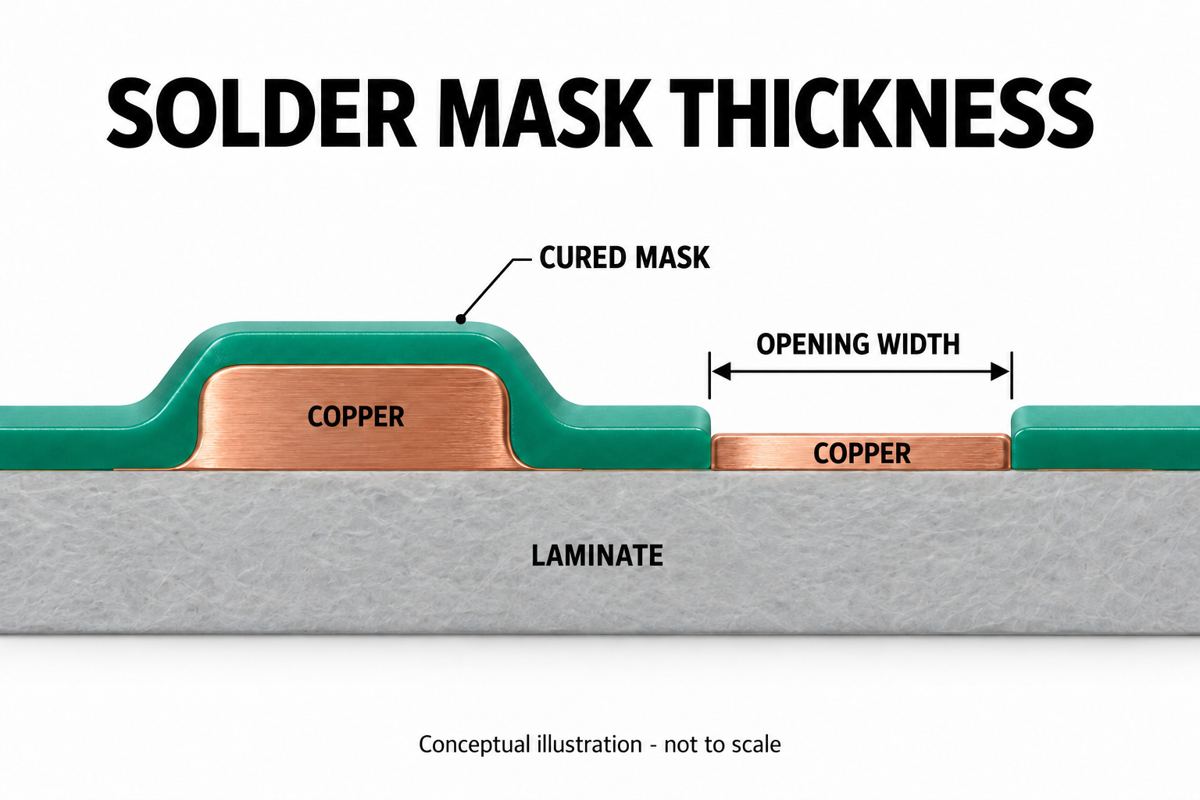
PCB solder mask thickness is the cured coating height at a defined location, not the width of a mask opening or the thickness of a solder-paste stencil. A useful specification identifies the underlying surface, the measurement datum and the acceptable limit. A single number without those details can describe several different measurements.
Before releasing a fine-pitch board, compare the component’s land-pattern requirements with the fabricator’s proposed coating and inspection method. The worksheet below helps you turn that comparison into a reviewable drawing note rather than an ambiguous request for “standard green mask.”
What does solder mask thickness mean?
Thickness describes a dimension through the coating. Clearance and dam width describe dimensions across the board. They need different checks even when all three are expressed in micrometers.
- Over-copper thickness: distance from the copper surface to the outside of its cured mask coverage at the specified location.
- Over-laminate thickness: coating above the exposed dielectric between copper features. Its bottom reference is not the top of a neighboring pad.
- Height relative to a land: how high nearby coating sits compared with the solderable land surface. This is not automatically the same as coating thickness.
- Mask opening or clearance: the lateral opening around a pad. A larger opening does not specify a thinner coating.
A coating can meet its over-copper thickness requirement while the opening is incorrectly registered. Conversely, a correct opening can surround a coating that violates a package-specific height limit. Review those failures separately. For lateral bridges between pads, see the separate solder mask dam and clearance guide.
How thick should solder mask be?
Use a location-specific range or limit agreed for the actual board and component, not a universal number copied from a capability page. The lower boundary addresses coverage; an upper boundary may be needed around a low-standoff package. A process also has to produce acceptable cure, adhesion and registration, none of which is proven by thickness alone.
For context, Eurocircuits’ microsection guidance states an 8 µm minimum over copper conductors. That is a published supplier criterion, not a statement of PCBtry capability or an automatic acceptance requirement for your purchase order. A device manufacturer can impose a different constraint for its footprint, as the example below shows.
Do not combine another fabricator’s minimum and a component’s maximum into an assumed production tolerance. Ask the selected fabricator whether the complete requirement can be controlled, where it will be measured, and how variation will be reported. If the two requirements cannot coexist, resolve the construction or package choice before fabrication.
What does TI specify for the TPA6166A2 PCB footprint?
The TPA6166A2 provides a concrete example of why coating height and opening size must remain separate. TI’s SLAS997B datasheet, page 42, Table 8 and footnote 5, gives the following WCSP land-pattern guidance.
| Parameter | Published value | How to use it |
|---|---|---|
| Land definition | NSMD | Copper defines the land; do not substitute a mask-defined footprint without approval. |
| Copper pad | 230 µm | Land dimension, not coating height. |
| Solder mask opening | 310 µm | Opening dimension; check registration independently. |
| Mask above the copper circuit pattern | Less than 20 µm | Package-specific upper limit at the stated surface. |
| Stencil opening | 275 µm × 275 µm, rounded corners | Paste deposition geometry, not solder mask geometry. |
| Stencil thickness | 100 µm | Separate assembly tooling dimension. |
These are layout recommendations, not electrical absolute-maximum ratings or guaranteed PCB manufacturing tolerances. The table does not assign a plus/minus tolerance to the listed nominal land dimensions. Confirm the applicable package revision and manufacturing allowances with the responsible engineers.
The practical lesson is simple: specifying a 100 µm stencil says nothing about whether the cured mask meets the separate under-20 µm requirement. Likewise, passing a coating check cannot establish correct paste volume. Keep the fabrication drawing and stencil approval linked to the same footprint revision.
How do you measure solder mask over copper?
First define the two surfaces being measured; only then select the measurement method. A photo showing green coverage is useful for appearance but does not establish a calibrated thickness value.
- Mark the locations. Identify board side, component area, conductor top and any edge location that needs separate evaluation. Include dense and isolated features if they are relevant to the requirement.
- Agree the sample. Decide whether the measurement will use a board, a representative coupon or both. A broad flat coupon may not represent the geometry beside a fine-pitch package.
- Set the datum. Distinguish coating above copper from coating above laminate and from height above a solderable land. Put a sketch or annotated section in the inspection instruction.
- Measure the finished condition. State that the reading concerns cured solder mask and identify the production stage. Do not compare a wet deposit measurement directly with a cured acceptance limit.
- Record individual readings. Retain locations, equipment calibration information, uncertainty where relevant, and supporting images. An average alone can conceal a local violation.
- Apply the agreed decision rule. Treat a borderline reading within measurement uncertainty as a review case; do not round it into compliance.
For a destructive check, microsection preparation exposes the coating and substrate boundaries. Sample preparation must preserve those boundaries: a damaged edge or poorly defined interface is a reason to improve the section, not to select a more favorable point. Stoneridge’s historical revision-16 procurement specification, section 4.2.4, illustrates why conductor tops, edges and planes may have distinct criteria. It is customer-specific guidance, not a substitute for your current agreed specification.
Microsection vs surface measurement: which should you use?
Choose by the feature you need to resolve. A fast surface reading is useful only when its reference and local geometry match the question.
| Approach | Useful for | Limit and release check |
|---|---|---|
| Prepared microsection | Seeing coating relative to a conductor, edge or dielectric in a selected section | Destructive and local. Identify the cut plane, preserve boundaries and agree sampling. |
| Validated surface-height method | Comparing accessible surface heights against a known reference | A height difference may include copper or finish. Show how the coating contribution is isolated. |
| Coating gauge on a suitable coupon | Repeatable process monitoring after method validation | Probe area, substrate and geometry must suit the instrument. Do not assume a coupon resolves a narrow conductor edge. |
| Visual inspection | Coverage, damage, contamination and obvious opening defects | Not a calibrated thickness measurement. Use alongside, not instead of, the agreed dimensional check. |
For a dispute, ask both parties to measure the same location with the same datum and specimen condition. If one report measures from laminate and the other from copper, the disagreement may be definitional rather than a process change. Correlate the methods before treating either result as the acceptance reference.
What should a solder mask inspection record include?
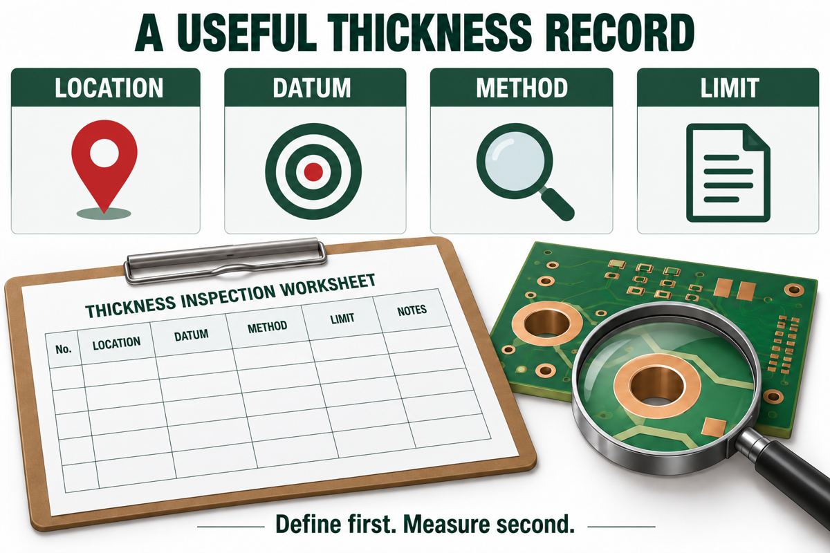
Use this worksheet before ordering and retain the completed version with the lot documentation. Blank or contradictory fields mean the requirement needs clarification, not that a default value should be guessed.
| Record field | What to enter | What it prevents |
|---|---|---|
| Board identity | Part number, revision, lot and side | Accepting results from another design or build. |
| Material and condition | Exact mask designation, cured condition and inspection stage | Comparing different formulations or wet and dry values. |
| Location and datum | Annotated feature coordinates and reference surface | Mixing edge coverage, over-copper thickness and land-relative height. |
| Requirement source | Drawing revision and component guidance where applicable | Using an unrelated supplier’s published range. |
| Acceptance limit | Agreed minimum/maximum or range, units and decision rule | Turning a nominal number into an invented tolerance. |
| Method and sampling | Section/gauge method, sample locations and agreed frequency | Assuming one flat reading covers every feature. |
| Results and disposition | Individual readings, images, deviations and authorized decision | Losing evidence behind a simple “pass” statement. |
Drawing-note starting point: “Report cured solder mask at locations [IDs], using datum [surface] and method [agreed method]. Acceptance limits [approved values and units] apply to [specified features]. Record individual results and obtain disposition for deviations before shipment.” Fill the brackets jointly; this template intentionally supplies no universal numerical limit.
If the concern is the production sequence rather than metrology, use the existing PCB solder mask overview. Keep this worksheet attached to the specific inspection task.
Solder mask thickness FAQ
Is solder mask thickness the same as solder mask clearance?
No. Thickness is a vertical coating dimension; clearance is the lateral relationship between copper and a mask opening. Changing clearance in CAD does not directly set the cured coating thickness. Send both the manufacturing data and any dimensional coating requirement, so the fabricator can review them separately.
Is a silkscreen line width a solder mask thickness?
No. A silkscreen line is a printed marking. Its line width does not describe the protective mask beneath it. When a drawing calls out “0.1 mm,” include the feature name and direction; otherwise a legitimate number can be assigned to the wrong manufacturing layer.
Does stencil thickness set solder mask thickness?
No. The stencil controls paste deposition during assembly; solder mask is part of PCB fabrication. Their numerical requirements can differ greatly. The TI footprint example separates the two, which is why a stencil approval should never be used as evidence that a cured mask requirement has passed.
Will thicker solder mask fix a narrow mask dam?
Not by itself. A dam is a lateral strip between openings. Its printability depends on the actual geometry and the fabricator’s process. Discuss opening dimensions, registration and the disposition of narrow strips. Do not approve a thicker coating as a substitute for checking the dam width.
Does nominal PCB thickness include the solder mask?
Do not assume it does or does not. The drawing and supplier agreement must define the finished-board measurement condition and reference surfaces. A nominal board thickness is not a measurement of the local coating above a trace. Keep overall-board thickness and solder-mask inspection as separate requirements.
Can I measure solder mask thickness with ordinary calipers?
A caliper across the entire PCB does not isolate the coating. Its reading includes the board construction and whichever surface features contact the jaws. Use a validated method that resolves the required local dimension; for fine features, request an appropriately prepared and calibrated cross-section report.
Does a darker solder mask prove that the coating is thicker?
No. Appearance depends on formulation, color, underlying features and illumination. Visual differences can identify locations worth checking, but they are not a substitute for dimensional measurement. Use the agreed material identity and inspection method rather than accepting or rejecting a batch by shade alone.
What should I do if measured thickness is near a limit?
Review the datum, calibration, uncertainty and sample preparation before disposition. Repeat or correlate the measurement using the agreed procedure where necessary. Do not change the limit after seeing the result or round away a nonconformance. Record the engineering decision and any approved deviation against the lot.
Request a solder mask specification review
Send the copper and solder mask manufacturing files, fabrication drawing, board revision, relevant component part numbers and the completed inspection worksheet through PCBtry’s contact page or email sales@pcbtry.com. Identify the locations that need controlled coating thickness and request confirmation of the proposed material, measurement method, limits and inspection scope before production approval.



0 Comments