




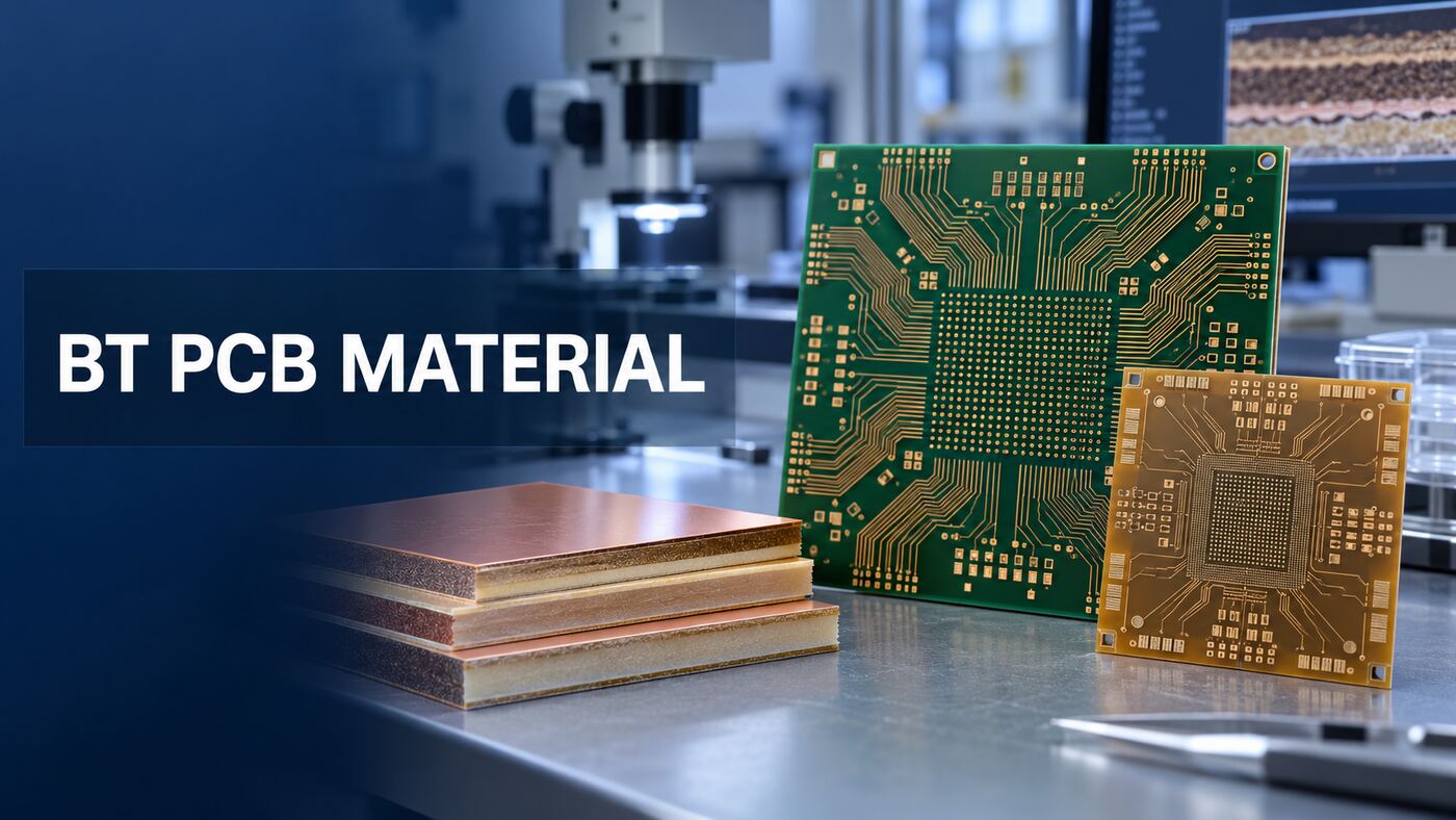
Bismaleimide-triazine, commonly called BT resin, is a high-performance thermosetting resin system used in electronic laminates and semiconductor package substrates. It is considered when a design needs stronger thermal stability, tighter dimensional control, favorable moisture behavior, or package-level interconnection performance beyond what a conventional laminate can provide.
BT is not one universal material grade. Its performance depends on the resin formulation, reinforcement, copper foil, laminate construction, cure process, and test method. Engineers should specify the required properties and construction rather than writing only “BT material” on a drawing or request for quotation.
What Is Bismaleimide-Triazine?
Bismaleimide-triazine is a thermosetting polymer resin system developed for demanding electronic laminates and packaging substrates. Commercial formulations may combine bismaleimide, triazine-forming chemistry, epoxy components, fillers, and reinforcing glass fabrics in different proportions.
During curing, these constituents form a highly cross-linked polymer network. Depending on the grade, the cured structure can provide high-temperature stability, electrical insulation, dimensional control, and resistance to moisture-related changes.
| Term | Practical Meaning | Why the Difference Matters |
| BT resin | The bismaleimide-triazine polymer system | It describes chemistry, not a complete production laminate. |
| BT prepreg | Partially cured BT-based resin combined with reinforcement | Resin content, flow, glass style, and cure behavior affect lamination. |
| BT laminate | Fully cured reinforced laminate, often supplied with copper cladding | The grade and construction determine available electrical and mechanical properties. |
| BT PCB | A printed circuit board fabricated with a BT-based laminate system | It may still use conventional PCB-scale design rules and processes. |
| BT substrate | Usually an organic semiconductor package substrate made with BT material | It may require much finer geometry and tighter warpage control than a PCB. |
| BT epoxy | A formulation that combines BT chemistry with epoxy constituents | Its properties depend on the complete formulation, not the BT name alone. |
Writing only “BT material” leaves important decisions undefined, including laminate grade, thickness, resin content, reinforcement, copper foil, glass-transition temperature, thermal expansion, dielectric properties, and dimensional requirements.
Why Is BT Used in PCBs and IC Substrates?
BT is used when thermal and dimensional stability directly affect interconnection reliability. These requirements become more important as conductors become finer, substrates become thinner, and package I/O density increases.
A fine-pitch BGA substrate may experience several thermal cycles during substrate fabrication, semiconductor packaging, and final SMT assembly. Excessive dimensional movement or warpage can affect registration, solder-joint coplanarity, and assembly yield. A suitable BT construction can provide additional process margin when compared with a general-purpose laminate.
- High glass-transition temperature in selected grades
- Controlled thermal expansion and dimensional movement
- Favorable moisture behavior
- Reliable electrical insulation
- Useful dielectric performance in appropriate formulations
- Stability during high-temperature fabrication and assembly
- Compatibility with fine-pitch package structures
- Established use in semiconductor package substrates
These advantages are grade dependent. The selected supplier datasheet, approved construction, and intended fabrication process should control the final material decision.
Which BT Material Properties Matter Most?
The most important properties are those that connect directly to the product’s electrical, thermal, mechanical, and manufacturing requirements.
| Property | Engineering Relevance | What to Verify |
| Glass-transition temperature (Tg) | Indicates the temperature region where polymer behavior changes | Test method, material grade, and whether the value is TMA, DSC, or DMA based |
| Coefficient of thermal expansion (CTE) | Helps predict dimensional movement and stress during heating and cooling | X-Y and Z-axis values, temperature range, and stackup influence |
| Dielectric constant (Dk) | Affects impedance, propagation delay, and transmission-line geometry | Test frequency, method, nominal Dk versus design Dk, and pressed thickness |
| Dissipation factor (Df) | Contributes to dielectric insertion loss | Frequency-specific data and a comparable test method |
| Moisture absorption | Influences storage, dimensional stability, and reflow risk | Conditioning method and supplier handling recommendations |
| Copper adhesion and copper profile | Affect conductor reliability and high-frequency loss | Available foil type, peel strength, roughness, and process compatibility |
| Resin flow and cure behavior | Affect lamination quality, thickness control, and void risk | Approved press cycle, glass style, resin content, and storage condition |
Generic values found online are only screening references. A dielectric value measured at one frequency or by one method should not automatically be entered into a field solver for a different frequency range. Use the selected laminate datasheet and confirm the design values used by the fabricator.
Is BT Better Than FR-4?
BT is not universally better than FR-4. It becomes useful when the chosen FR-4 grade cannot provide enough thermal, dimensional, moisture, or package-level performance.
FR-4 is a material classification rather than one fixed performance level. High-Tg, low-loss, and low-CTE FR-4-family laminates can support many demanding multilayer PCBs.
| Decision Factor | Standard or High-Tg FR-4 | BT Material |
| Material cost | Usually lower | Usually higher |
| Supply availability | Broad | More specialized and grade dependent |
| Conventional multilayer PCB | Often the preferred choice | May be unnecessary |
| Thermal and dimensional stability | Grade dependent | A common reason to evaluate BT |
| BGA/CSP package substrate | Limited in demanding structures | Established application |
| Fabrication experience | Widely available | Requires a BT-capable material and process supply chain |
For an ordinary industrial control board, a suitable FR-4 grade may provide the best balance of performance, availability, and cost. BT becomes more compelling for package substrates, fine-pitch interconnections, and structures with tighter thermomechanical limits.
The practical question is not “Is BT better than FR-4?” It is: Does this stackup require performance that the selected FR-4 grade cannot reliably provide?
Where Is BT Material Used?
BT is most strongly associated with semiconductor package substrates and selected high-density interconnection structures.
- BGA and CSP substrates
- Memory packages
- Semiconductor and RF modules
- MEMS and image-sensor packages
- Chip LED and communication electronics
- Automotive electronic modules with suitable qualification
- High-density multilayer circuits
- High-frequency products using a verified low-loss BT grade
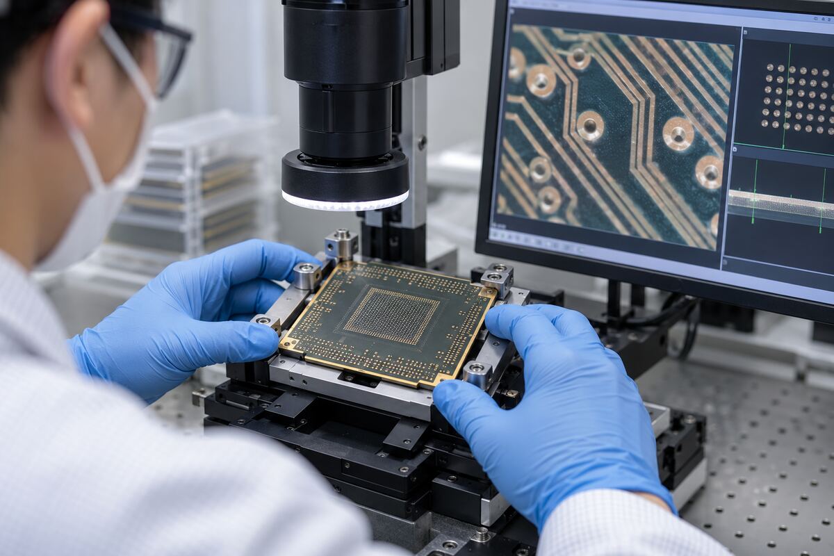
In a BGA package, the substrate redistributes fine connections near the semiconductor die to the larger solder-ball array that connects to the system PCB. The substrate is therefore part of the semiconductor package interconnect, not simply a small version of a motherboard.
What Is the Difference Between a BT Substrate and a BT PCB?
A BT substrate usually means an IC package substrate, while a BT PCB generally means a printed circuit board manufactured with a BT-based laminate. The difference is mainly function, geometry, and manufacturing scale.
Semiconductor die → BT package substrate → BGA solder balls → system PCB
This distinction can change the required conductor width and spacing, microvia diameter, layer construction, pad pitch, registration tolerance, finished thickness, flatness, warpage control, surface finish, inspection method, and reliability qualification.
When a drawing says “BT substrate,” the supplier should confirm whether the customer needs a true semiconductor package substrate or a conventional PCB made from BT laminate. Clarifying this point early can prevent major quotation and manufacturing errors.
BT vs ABF: How Are They Different?
BT is a strong fit for many established BGA, CSP, memory, and module packages. ABF is an interlayer build-up film used where package substrates require very fine routing, laser processing, and high I/O density.
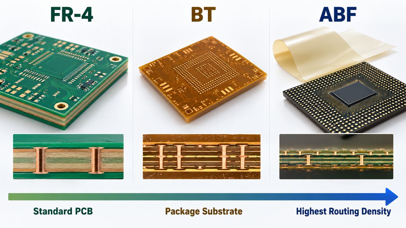
| Design Factor | BT-Based Substrate | ABF Build-Up Structure |
| Mature BGA/CSP and memory packages | Strong fit | Application dependent |
| Very high-I/O processor packages | Geometry may become limiting | Widely used for dense build-up routing |
| Material form | Often a reinforced laminate system | Thermosetting build-up dielectric film |
| Fine routing and microvias | Process and grade dependent | Designed to support laser processing and direct copper plating |
| Main selection drivers | Reliability, routing, package type, availability, and cost | High routing density, I/O count, and package architecture |
BT and ABF are not always direct substitutes for a complete substrate. A package may use several materials, and ABF can describe only its build-up dielectric layers. Start with die size, I/O count, pad pitch, required line/space, via architecture, layer count, package size, and warpage limit before choosing the material system.
What Manufacturing Risks Should Be Reviewed?
The main risks are material substitution, stackup availability, lamination behavior, drilling, registration, moisture control, copper adhesion, and warpage.
Material Substitution
Changing to another BT grade can alter Tg, CTE, Dk, Df, resin flow, copper adhesion, and available thicknesses. Substitutions should require approval when impedance, dimensional stability, or package reliability is critical.
Stackup and Lamination
A theoretical stackup may use cores or prepregs that the selected manufacturer cannot source. Resin flow, cure profile, pressure, copper balance, and pressed thickness all affect the finished construction. Obtain a manufacturable stackup before final routing.
Drilling and Microvias
Mechanical drilling, laser drilling, blind vias, buried vias, and via-in-pad structures impose different material and process requirements. Agree on the via architecture before releasing the material specification.
Warpage and Registration
Thin substrates, asymmetric copper, and unbalanced stackups can distort during thermal processing. Fine-pitch packages may have tight coplanarity and registration limits, so copper balance and stackup symmetry need early review.
Moisture and Storage
Favorable moisture performance does not remove the need for controlled storage and handling. Follow the material supplier’s shelf-life, storage, bake, and processing recommendations.
Copper Profile and Signal Loss
Copper roughness affects both conductor adhesion and high-frequency loss. For high-speed or RF designs, evaluate copper profile together with Dk, Df, trace geometry, dielectric thickness, and routing length.
How Should Engineers Select a BT Material?
Select the material backward from the finished product requirements rather than forward from the resin name.
- Define the operating temperature range.
- Identify the assembly and reflow profile.
- Define the board or package dimensions.
- Specify finished thickness and tolerance.
- Establish minimum line/space.
- Define via type and minimum via size.
- Identify fine-pitch BGA or CSP requirements.
- Set controlled-impedance targets.
- Define frequency and acceptable insertion loss.
- Establish flatness or warpage limits.
- Define environmental and reliability testing.
- Confirm available BT grades and constructions with the manufacturer.
For high-speed designs, ask which test method and frequency were used for Dk and Df, whether the published value is nominal or intended for design, which copper foil profiles are available, what pressed dielectric thickness will be used, and what impedance tolerance the fabricator can maintain.
IPC-4101E-WAM1 covers requirements for laminate and prepreg base materials used primarily for rigid and multilayer printed boards. IPC-6012F establishes qualification and performance requirements for rigid printed boards. Confirm the applicable revision, specification sheet, product class, addendum, and customer requirements for each project.
Can BT Be Used for High-Frequency PCBs?
Selected BT formulations can support high-frequency PCB applications, but the words “BT resin” alone do not guarantee low loss.
Total signal loss depends on Dk and Df at the relevant frequency, copper roughness, conductor geometry, dielectric thickness, glass reinforcement, routing length, and fabrication variation. Recent materials research continues to modify BT systems for lower dielectric loss, but experimental resin data should not be treated as the guaranteed performance of a commercial laminate.
Use the actual laminate datasheet and the fabricator’s production stackup. If insertion loss is critical, compare candidate materials using data measured at relevant frequencies and by comparable methods. High Tg and low loss are different properties: a thermally robust material is not automatically the best dielectric for a high-frequency channel.
How Does BT Affect PCB and Package Reliability?
BT can improve reliability when its properties match the package, stackup, via design, assembly profile, and operating environment.
During fabrication and use, copper, resin, reinforcement, silicon, and solder joints expand at different rates. Repeated temperature changes can concentrate stress around vias, microvias, copper interfaces, BGA joints, package corners, and thin dielectric regions.
A suitable BT construction can help control thermomechanical movement, but material choice alone does not guarantee reliability. Review Tg, CTE, moisture performance, copper adhesion, stackup symmetry, copper balance, via geometry, warpage, inspection evidence, and qualification testing as one system.
What Should Be Included in a BT PCB RFQ?
A useful RFQ should specify the required construction and performance rather than only stating “use BT.”
- Gerber or ODB++ files and fabrication drawing
- Intended application and package type
- Layer count and proposed stackup
- Finished dimensions, thickness, and tolerance
- Requested BT grade or approved-equivalent rules
- Copper thickness and foil-profile requirements
- Controlled-impedance and insertion-loss targets
- Minimum line/space and finished-hole size
- Blind, buried, microvia, or via-in-pad requirements
- Surface finish and solder-mask requirements
- Warpage or flatness limit where critical
- Electrical test, inspection, and reliability requirements
- Prototype and production quantities
If the exact laminate has not been selected, define measurable performance targets and require approval before substitution. A complete data package produces a more useful DFM response than a request for “BT PCB” alone.
Frequently Asked Questions
What is bismaleimide-triazine?
Bismaleimide-triazine is a high-performance thermosetting resin system used in electronic laminates and semiconductor package substrates. Depending on its formulation and reinforcement, it can provide useful thermal stability, electrical insulation, moisture resistance, and dimensional control.
What does BT material mean in a PCB?
BT material usually means a laminate or prepreg based on bismaleimide-triazine resin. It does not identify one universal grade. The drawing or RFQ should also define the selected grade or required Tg, CTE, Dk, Df, thickness, copper foil, and dimensional performance.
Is BT better than FR-4?
Not for every design. BT is attractive when a project requires package-substrate capability or stronger thermal and dimensional performance. A suitable high-Tg or low-loss FR-4-family laminate may remain more economical and widely available for a conventional multilayer PCB.
What is the difference between a BT substrate and a BT PCB?
A BT substrate normally refers to an IC package substrate that connects a semiconductor die to the package interface. A BT PCB is generally a printed circuit board fabricated from BT laminate. The substrate may require finer lines, smaller microvias, tighter registration, and stricter warpage control.
What is the difference between BT and ABF?
BT is commonly used as a reinforced laminate system in established BGA, CSP, memory, and module substrates. ABF is a build-up dielectric film used for fine routing and laser processing in many high-I/O package substrates. They are not necessarily direct substitutes within a complete construction.
Does BT resin have a high Tg?
Many BT systems are designed for high thermal stability, but Tg varies by formulation and test method. Use the selected laminate’s datasheet rather than a generic BT value, and confirm how the value was measured.
Is BT suitable for high-frequency PCB applications?
Some BT grades are suitable, but selection must use frequency-specific Dk, Df, and loss data. Copper roughness, dielectric thickness, trace geometry, reinforcement, and fabrication variation also affect insertion loss.
What causes warpage in a BT substrate?
Common contributors include thin construction, asymmetric copper distribution, unbalanced stackups, resin cure behavior, material CTE mismatch, and thermal-process variation. Warpage control should begin during stackup and copper-balance review.
Can one BT grade replace another?
Not automatically. Different grades may have different thermal, dielectric, resin-flow, copper-adhesion, thickness, and availability characteristics. Any substitution affecting performance or manufacturability should be documented and approved.
What files are needed for a BT PCB quotation?
Provide Gerber or ODB++ data, a fabrication drawing, stackup, dimensions, thickness tolerance, copper requirements, impedance targets, via structure, surface finish, quantities, and any flatness, inspection, reliability, or qualification requirements.
When Should You Choose Bismaleimide-Triazine?
Choose BT when measurable electrical, thermal, dimensional, or package-level requirements justify its material and process constraints.
FR-4 remains appropriate for a large share of conventional printed circuit boards. ABF becomes more attractive as package routing moves toward very fine build-up structures and high I/O counts. BT occupies an important engineering space where package-substrate experience, thermal stability, and dimensional reliability are valuable.
If your project involves a BT PCB, package-substrate-like construction, fine-pitch BGA routing, or controlled impedance, send the Gerber or ODB++ files, stackup, drawings, material targets, tolerances, and quantities to sales@pcbtry.com or use the PCBTRY contact form. The engineering review should confirm material availability, manufacturable geometry, stackup, and testing before quotation or production.
References
- Mitsubishi Gas Chemical: BT Laminate—Products and Technology Highlights
- Mitsubishi Gas Chemical: BT Materials and IC Package Substrates
- Ajinomoto: Ajinomoto Build-up Film (ABF)
- IPC: IPC-4101E-WAM1 and IPC-6012F Standard Summaries
- Journal of Materials Chemistry C: Modified BT Resin for High-Frequency Electronic Packaging



0 Comments