
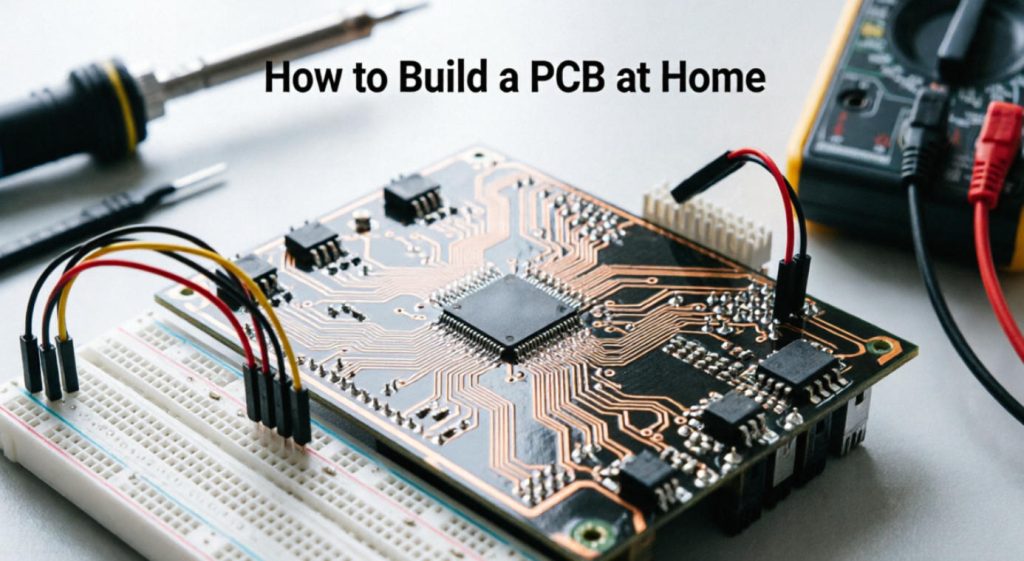
Building a PCB at home means turning a circuit design into a physical copper board using basic tools, a blank copper-clad laminate, a pattern transfer method, etching, drilling, soldering, and electrical testing. It is practical for simple one-sided circuits, quick experiments, and learning how PCB design really works, but it has clear limits in trace width, hole plating, solder mask, repeatability, and safety control.
If you are making your first homemade PCB, start small: one layer, through-hole components, wide traces, generous spacing, and a circuit you can test section by section. Once the design needs fine-pitch ICs, controlled impedance, multilayer routing, ENIG surface finish, high current, medical reliability, automotive compliance, or production repeatability, it is usually time to move from home fabrication to professional PCB prototyping.
What Is a Homemade PCB?
A homemade PCB is a custom circuit board fabricated outside a professional PCB factory, usually on a single-sided or double-sided copper-clad board using manual transfer, chemical etching, mechanical drilling, and hand soldering.
The basic idea is simple. You design the circuit on a computer, print or expose the copper pattern, remove unwanted copper, drill component holes, then solder the parts. For hobby circuits, sensor modules, LED projects, simple power boards, audio experiments, Arduino shields, and classroom demonstrations, this can work surprisingly well.
However, a home-built board is not the same as a factory-made PCB. Professional boards are produced with controlled lamination, CNC drilling, plated through holes, solder mask, silkscreen, copper thickness control, impedance testing, electrical test, and quality standards such as IPC-A-600 and IPC-A-6012. At home, most of that process is simplified or missing.
Why Build a PCB at Home Instead of Using a Breadboard?
A home-built PCB gives your circuit stronger mechanical stability, cleaner wiring, and a more realistic prototype than a breadboard.
Breadboards are convenient for early experiments, but they become unreliable when the circuit grows. Jumper wires loosen, parasitic capacitance increases, grounding becomes messy, and high-current paths are difficult to manage. A PCB forces you to think about layout, current flow, component placement, connector orientation, and test points.
For learning, this is the real value. You begin to see why a power trace should be wider, why decoupling capacitors belong close to IC power pins, why ground routing matters, and why a schematic that works in simulation may fail when placed on a poor layout.
At the same time, home fabrication is best treated as an engineering learning tool, not a replacement for controlled manufacturing. If the board will be sold, installed in a customer product, used near high voltage, or placed in a safety-critical system, a professional prototype run is the safer path.
How a PCB Works in Simple Terms
A PCB works by replacing loose wires with copper traces bonded to an insulating base material, allowing electrical signals and power to travel between components in a fixed, repeatable layout.
The most common PCB base material is FR-4, a glass-reinforced epoxy laminate. On top of it sits a thin copper layer. During fabrication, unwanted copper is removed, leaving only the traces, pads, and copper areas needed by the circuit. Components are then soldered to the copper pads.
A simple homemade PCB normally has one copper layer. A double-sided board has copper on both sides, but connecting the two sides at home is not as straightforward as in a factory because plated through holes are not usually available. Hobbyists often use small wire links or rivets to connect top and bottom layers, but this adds manual work and reduces repeatability.
PCB Building Methods You Can Use at Home
The easiest home PCB methods are toner transfer, photoresist exposure, CNC isolation routing, and marker-based manual drawing, each with different accuracy, cost, and learning curve.
| Method | Best For | Relative Cost | Limitations |
|---|---|---|---|
| Toner Transfer | Simple one-sided boards, beginner projects | Low | Depends heavily on printer quality, heat, pressure, and surface cleaning |
| Photoresist PCB | Cleaner traces and more repeatable DIY results | Medium | Requires UV exposure control, developer, and better process discipline |
| CNC Isolation Routing | Fast chemical-free prototypes | Medium to high | Needs a CNC machine, sharp bits, flat board setup, and dust control |
| Permanent Marker | Very rough experiments or emergency repairs | Very low | Poor accuracy, not suitable for dense layouts or repeatable results |
For most beginners searching how to build a PCB at home, toner transfer is the usual starting point. It needs fewer tools than photoresist and does not require a CNC machine. If you plan to make several boards and want cleaner results, photoresist is worth learning. If you dislike chemicals and already have access to a desktop CNC, isolation routing can be efficient, especially for same-day prototypes.
Tools and Materials You Need Before Starting
You need design software, copper-clad laminate, a transfer or exposure method, etching or routing equipment, drilling tools, soldering tools, cleaning supplies, and basic electrical test equipment.
For the design stage, KiCad, EasyEDA, Altium Designer, and Eagle are commonly used. KiCad is especially popular for hobby and engineering learning because it is capable, free, and widely documented. For the board material, beginners usually choose single-sided FR-4 copper-clad laminate. FR-1 phenolic board is easier to drill but less mechanically and thermally robust than FR-4.
A typical toner-transfer setup includes a laser printer, glossy transfer paper or dedicated toner-transfer paper, a laminator or iron, copper-clad board, fine abrasive pad, acetone or isopropyl alcohol for cleaning, an etchant such as ferric chloride or sodium persulfate, plastic containers, drill bits, a small drill press or rotary tool, solder wire, flux, and a multimeter.
Use chemical-resistant gloves, eye protection, ventilation, and clearly labeled containers when handling etchants or cleaning chemicals. Never mix chemicals casually, never pour used etchant into household drains, and follow local disposal regulations.
Design the Circuit Before You Touch the Copper
A reliable homemade PCB starts with a simple schematic, correct footprints, wide traces, realistic spacing, and a layout that respects the limits of home fabrication.
Do not begin by drawing copper traces directly unless the circuit is extremely simple. Create a schematic first, assign real component footprints, then move into board layout. Print the layout on paper at 1:1 scale and place the actual components on top. This catches many beginner mistakes: wrong pin pitch, reversed connectors, too-small pads, missing mounting holes, and components that collide physically.
For home etching, use conservative design rules. Wide traces are easier to transfer and survive etching better. Generous spacing reduces the chance of copper bridges. Large pads make drilling and soldering more forgiving. If your circuit allows it, use through-hole components rather than fine-pitch SMD parts for the first few boards.
| Design Parameter | Home PCB Recommendation | Why It Helps |
|---|---|---|
| Trace Width | Use wider traces where space allows | Improves etching tolerance and current handling |
| Trace Spacing | Keep spacing generous | Reduces shorts caused by transfer defects or under-etching |
| Pad Size | Use larger pads for drilled holes | Prevents pads from lifting or disappearing after drilling |
| Layer Count | Start with one layer | Avoids alignment and via connection problems |
| Silkscreen | Print an assembly drawing separately | Homemade boards usually do not include real silkscreen |
Step-by-Step: How to Build a PCB at Home
The practical process is to design the board, transfer the pattern, etch away unused copper, drill the holes, clean the board, solder the components, and test each connection before applying full power.
Prepare the PCB Layout
Export the copper layer as a mirrored image if you are using toner transfer for the bottom layer. Check that the scale is exactly 1:1. Disable printer scaling, fit-to-page settings, or any automatic resizing. A small printing error can make IC footprints unusable.
Clean the Copper Surface
Scrub the copper surface lightly with a fine abrasive pad until it looks even and bright. Remove grease with isopropyl alcohol or another suitable cleaner. Fingerprints are a common reason toner does not stick properly.
Transfer the Pattern
Place the printed toner pattern against the copper and apply controlled heat and pressure using a laminator or iron. The goal is to bond the toner to the copper without smearing fine traces. Let the board cool before removing the paper. If the transfer has missing pads or broken traces, clean the board and repeat instead of trying to rescue a bad transfer.
Etch the Board
Place the board in the etchant according to the chemical supplier’s instructions. Agitate gently and monitor progress. Remove the board once unwanted copper is gone. Over-etching can narrow traces and weaken pads. Rinse the board carefully in a controlled area and handle used solution as chemical waste.
Remove Toner and Inspect
Remove the toner or resist layer after etching. Inspect the copper under good lighting. Look for hairline breaks, copper bridges, thin traces, and pads that look partially etched. A magnifier helps. Repair small breaks with solder bridges or wire jumpers only if the defect is minor and the circuit is low risk.
Drill the Holes
Use sharp carbide or high-speed steel micro drill bits and keep the board flat. Drill slowly and vertically. FR-4 is abrasive and can dull bits quickly. Wear eye protection and control dust. Misaligned drilling is one of the biggest problems in homemade through-hole boards, so large pads make life easier.
Solder the Components
Start with low-profile components such as resistors and diodes, then sockets, capacitors, connectors, and larger parts. Check polarity before soldering diodes, electrolytic capacitors, ICs, LEDs, and voltage regulators. Use flux and avoid overheating pads, especially on cheaper laminate.
Test Before Full Power
Use a multimeter to check continuity, shorts between power rails, correct resistor values, and diode orientation. If the board includes a power supply section, test it without sensitive ICs installed if possible. Bring up the board gradually using a current-limited supply when available.
Common Beginner Mistakes That Ruin Homemade PCBs
Most failed homemade PCBs come from poor layout preparation, dirty copper, printer scaling errors, thin traces, over-etching, drilling misalignment, or skipping continuity tests.
The most painful mistake is discovering that the layout was not mirrored correctly after etching. The second is printing at the wrong scale. Always verify by placing real components on a paper printout before transferring anything to copper.
Another common issue is using traces and clearances that look normal on a professional PCB but are too fine for a first home process. A factory can hold tight tolerances because imaging, etching, plating, solder mask, and inspection are controlled. At home, every step has more variation. Design with that reality in mind.
Beginners also underestimate drilling. A pad that looks large on-screen may be too small once the drill wanders slightly. If a pad lifts during soldering, the electrical connection becomes weak even if the joint looks acceptable.
Testing and Troubleshooting a Homemade PCB
Testing should begin before soldering and continue after each assembly stage, because finding one defect early is much easier than debugging a fully populated board.
After etching, check every trace that carries power or a critical signal. Use continuity mode to verify that connected pads are actually connected. Then check for unwanted shorts between adjacent pads, IC pins, power rails, and connector terminals.
After soldering, inspect joints under magnification. A good solder joint usually looks smooth and slightly concave. Dull, cracked, or ball-shaped joints may indicate poor wetting or insufficient heat. For ICs, check bridges between pins. For power circuits, check polarity twice before powering up.
| Symptom | Likely Cause | What to Check First |
|---|---|---|
| No power on the board | Broken power trace, reversed connector, bad solder joint | Input connector, fuse, regulator pins, continuity from supply |
| Power supply shuts down | Short circuit between power and ground | Rail resistance, solder bridges, reversed capacitor |
| IC gets hot quickly | Wrong orientation, shorted output, incorrect voltage | Pin 1 position, supply voltage, neighboring solder bridges |
| Signal is unstable | Poor grounding, long traces, missing decoupling | Ground return path, capacitor placement, connector wiring |
| Intermittent operation | Cracked trace, lifted pad, weak solder joint | Mechanical stress points, connector pads, drilled holes |
Materials Used in DIY and Professional PCBs
DIY PCBs usually use simple copper-clad FR-4 or phenolic laminate, while professional PCB manufacturing offers controlled base materials, copper weights, solder masks, surface finishes, and specialty laminates.
For home projects, single-sided FR-4 is the most practical choice when durability matters. Phenolic paper laminate is easier to cut and drill, but it is less suitable for heat, vibration, or long-term use. Copper thickness on common hobby laminate is often around 1 oz, but exact specifications should be checked from the material supplier.
Professional boards can be built from standard FR-4, high-Tg FR-4, aluminum substrate, copper substrate, Rogers or Taconic high-frequency materials, flexible polyimide, rigid-flex stackups, and thick copper structures. The right material depends on heat, frequency, current, mechanical bending, operating environment, and compliance requirements.
That difference matters when a prototype leaves the bench. A LED lighting board may need an aluminum PCB for heat dissipation. An automotive BMS board may need thick copper, high reliability, and wide-temperature performance. A 5G RF module may need low-loss high-frequency laminate and controlled impedance. These are not realistic targets for home fabrication.
When a Home PCB Is Good Enough
A home-built PCB is good enough when the circuit is low voltage, low complexity, non-critical, easy to inspect, and built mainly for learning, experimentation, or a one-off prototype.
Good candidates include LED blinkers, small sensor boards, simple audio circuits, relay interface boards, educational microcontroller projects, battery-powered hobby devices, and adapter boards with relaxed tolerances. These projects can tolerate manual rework and do not usually require certification-grade consistency.
Home PCBs are less suitable for mains power, medical electronics, automotive control, high-current converters, high-frequency RF, high-speed digital interfaces, dense BGA packages, and anything that must be produced repeatedly with stable quality. In those cases, the cost of one failure can be much higher than the cost of ordering a professional prototype.
When to Use Professional PCB Prototyping Instead
Professional PCB prototyping becomes the better choice when your design needs accuracy, plated through holes, solder mask, fine traces, multilayer routing, controlled impedance, surface finish control, assembly service, or repeatable production quality.
At Thindry, PCB prototyping and fabrication are built around a digitalized one-stop electronics workflow: EDA support, PCB manufacturing, components sourcing, and PCBA assembly. That matters when a project moves beyond a handmade experiment and needs engineering review, BOM optimization, SMT assembly, THT assembly, mixed-technology assembly, quality monitoring, and traceable production.
For buyers in the United States and other global markets, the practical concern is not only unit price. Engineers need boards that match design intent. Procurement teams need stable lead times, documented quality, and a supplier that can move from prototype to production without changing the manufacturing baseline. As a China-based source factory and global PCB/PCBA supplier, Thindry supports prototype runs, custom engineering requirements, and volume manufacturing without claiming local overseas factories or warehouses.
Quality Standards That Matter for Real PCB Projects
Quality standards matter because a PCB is not judged only by whether it works once, but by whether it can be manufactured, assembled, inspected, and used reliably over time.
For professional production, IPC standards are widely used across the PCB industry. IPC-A-600 covers acceptability of printed boards, while IPC-A-610 is commonly used for acceptability of electronic assemblies. UL recognition is relevant for safety-focused applications. RoHS compliance matters for restricted hazardous substances in many markets. ISO 9001 supports quality management systems, ISO 13485 applies to medical device quality systems, and IATF 16949 is used in automotive quality management.
Thindry’s manufacturing capability is positioned around globally recognized quality expectations, including ISO 9001, ISO 13485, IATF 16949, UL certified PCBs, and RoHS compliance. For any regulated product, the exact document package, test plan, and compliance evidence should be confirmed before production.
| Standard or Certification | Why It Matters | Typical Relevance |
|---|---|---|
| ISO 9001 | Quality management system | General PCB and PCBA manufacturing |
| ISO 13485 | Medical device quality management | Medical electronics and healthcare devices |
| IATF 16949 | Automotive quality management | Automotive electronics and EV systems |
| UL Certified PCBs | Safety-related board recognition | Power, industrial, lighting, and consumer electronics |
| RoHS Compliance | Restriction of hazardous substances | Products sold into RoHS-regulated markets |
Industry Applications Where DIY Is Not Enough
Home PCB fabrication is useful for learning, but commercial industries usually require controlled materials, tested manufacturing processes, and documented quality systems.
Consumer electronics often push PCB designs toward thin, compact, high-density structures such as HDI, FPC, and rigid-flex boards. Automotive electronics need higher reliability, vibration resistance, wide temperature performance, heat dissipation, and long service life. New energy vehicle systems such as BMS, VCU, MCU, and OBC boards often use thick copper, HDI, metal substrate, or high-reliability multilayer designs.
Communication equipment, including 5G infrastructure, routers, optical modules, RF front ends, and servers, may require high-frequency or high-speed materials, controlled impedance, high layer counts, and low insertion loss. AI servers and data center hardware place even higher demands on multilayer PCB stackups, signal integrity, thermal control, and flatness.
Industrial automation boards must survive electrical noise, temperature variation, vibration, and long operating hours. Medical electronics require precision, low noise, reliability, and compliance discipline. LED lighting boards depend heavily on thermal design, often using aluminum or copper substrates. Renewable energy and power electronics need high voltage, high current, heat management, and corrosion resistance.
These are exactly the places where the gap between “a board that works on my desk” and “a board that survives real use” becomes obvious.
Cost Factors: Home PCB vs Professional PCB Manufacturing
Home PCB cost looks low at first, but the real cost includes failed attempts, manual labor, tools, chemicals, rework, inconsistent yield, and the risk of design decisions that do not scale into production.
If you only need one simple board for learning, home fabrication can be inexpensive. But once you need several identical boards, solder mask, plated holes, surface mount assembly, reliable connectors, or repeatable dimensions, professional fabrication often becomes more economical.
| Cost Factor | Home PCB Impact | Professional PCB Impact |
|---|---|---|
| Setup Time | High manual preparation and trial-and-error | Front-loaded CAM review and production setup |
| Material Waste | Can be high during learning | Controlled panelization and process yield |
| Hole Quality | Manual drilling, no standard plated through holes | CNC drilling and plated vias available |
| Solderability | Bare copper oxidizes quickly | HASL, ENIG, OSP, immersion silver, or other finishes |
| Repeatability | Depends on operator skill | Controlled manufacturing and inspection |
| Assembly | Hand soldering only | SMT, THT, and mixed assembly options |
For a serious prototype, the best workflow is often hybrid: build the first crude version at home if it helps you understand the circuit, then send revised Gerber files for professional prototype manufacturing before investing in components, enclosures, compliance testing, or pilot production.
Procurement Checklist Before Ordering a Professional PCB
Before ordering a professional PCB, confirm the Gerber files, drill files, stackup, board thickness, copper weight, solder mask, surface finish, quantity, test requirements, assembly files, and compliance needs.
A clean file package saves time and prevents manufacturing questions. At minimum, prepare Gerber files, NC drill files, BOM, pick-and-place file for assembly, schematic if engineering review is needed, and any special notes about impedance, material, panelization, tolerances, or inspection requirements.
For PCBA projects, double-check component availability early. A board design that looks complete can still be delayed by one obsolete IC, long-lead connector, or incorrectly specified package. BOM optimization is not only about lowering cost; it also reduces sourcing risk and assembly problems.
- Confirm all footprints against real datasheets.
- Mark polarity clearly for diodes, LEDs, electrolytic capacitors, and ICs.
- Define board thickness and copper weight based on current and mechanical needs.
- Choose surface finish according to solderability, shelf life, and assembly type.
- Specify impedance control if the design includes high-speed signals.
- Confirm testing needs, such as electrical test, AOI, functional test, or custom test fixtures.
- Ask whether design-for-manufacturing feedback is available before production.
FAQ
Can I really build a PCB at home?
Yes, you can build a simple PCB at home using copper-clad laminate, a layout transfer method, etching or CNC routing, drilling, soldering, and a multimeter for testing. It is best for one-sided, low-voltage, low-density circuits. It is not ideal for fine-pitch components, plated vias, multilayer routing, high-speed signals, or products that require certification and repeatable production quality.
What is the easiest way to make a PCB at home?
For most beginners, toner transfer is the easiest method because it uses common tools such as a laser printer, transfer paper, heat, and a basic etching process. The results depend heavily on clean copper, correct print scaling, enough heat and pressure, and a layout designed with wide traces and generous spacing. Photoresist gives cleaner results but requires more process control.
Can I make a double-sided PCB at home?
You can make a double-sided PCB at home, but alignment and interlayer connections are difficult. Professional double-sided boards use plated through holes to connect layers. At home, you usually need wire links, rivets, or soldered jumpers. For simple circuits this may work, but dense layouts, fine-pitch ICs, and repeated builds are much better handled by professional PCB prototyping.
What software should I use to design a homemade PCB?
KiCad, EasyEDA, Eagle, and Altium Designer are common PCB design tools. KiCad is a strong choice for beginners and engineers who want a capable free tool. The most important point is not the software name, but whether you use correct footprints, generate proper Gerber files, check design rules, and print a 1:1 paper test before making the board.
Is it safe to etch PCBs at home?
PCB etching can be done safely only with proper precautions. Use eye protection, chemical-resistant gloves, ventilation, labeled containers, and a dedicated work area away from children, pets, food, and metal surfaces. Follow the chemical supplier’s instructions and local disposal rules. Used etchant should not be poured into household drains. If you cannot handle chemicals responsibly, use CNC routing or order a prototype board.
Why did my toner transfer PCB fail?
Common causes include dirty copper, wrong paper, insufficient heat, uneven pressure, printer toner that does not transfer well, or removing the paper too aggressively. Scaling errors and overly thin traces also cause trouble. Clean the copper thoroughly, verify the layout at 1:1 scale, use wider traces, and inspect the transfer before etching. If the pattern is badly broken, restart instead of etching it.
How do I stop traces from being over-etched?
Over-etching happens when the board stays in the etchant too long or the resist pattern is weak. Use fresh process control, monitor the board frequently, agitate gently, and remove it once unwanted copper is gone. Designing wider traces gives extra margin. If very fine traces are required, a home etching process may not be reliable enough, and professional fabrication is the better option.
Can homemade PCBs handle high current?
Homemade PCBs can handle some current if traces are wide enough and copper thickness is suitable, but the margin is often uncertain because material specifications, etching quality, solder coverage, and heat dissipation are not tightly controlled. For power electronics, motor drivers, EV systems, LED lighting, or high-current industrial boards, use professional PCB manufacturing with defined copper weight and thermal design review.
Do homemade PCBs need solder mask?
A homemade PCB can work without solder mask, but exposed copper oxidizes and solder bridges are more likely during assembly. Solder mask improves insulation, soldering control, durability, and appearance. Most DIY boards skip true solder mask or use simplified coating methods. For boards that need reliable assembly, long shelf life, or a professional finish, factory-applied solder mask is strongly recommended.
What is the difference between a homemade PCB and a prototype PCB from a factory?
A homemade PCB is manually made and usually lacks plated through holes, solder mask, controlled finish, electrical testing, and manufacturing documentation. A factory prototype PCB can include CNC drilling, copper plating, solder mask, silkscreen, surface finish, impedance control, multilayer stackups, and inspection. Home PCBs are useful for learning; factory prototypes are better for engineering validation and production planning.
When should I stop making PCBs at home and order professionally?
Order professionally when the board needs fine traces, small SMD parts, plated vias, multiple layers, controlled impedance, high current, high voltage, thermal performance, compliance documentation, or repeatable quality. Also order professionally if the design will be sold, used by customers, installed in equipment, or assembled in quantity. A low-cost prototype run can prevent many expensive reliability problems later.
Can Thindry help turn my homemade PCB into a production board?
Yes. If you already have a working homemade PCB, Thindry can help review the design for manufacturability, improve layout details, fabricate prototype boards, source components, and provide SMT, THT, or mixed PCBA assembly. This is especially useful when moving from a one-off bench project to a stable prototype, pilot run, or mass production order with documented quality requirements.
Final Thoughts
Building a PCB at home is one of the best ways to understand how electronic design becomes physical hardware. Keep the first board simple, use conservative design rules, inspect every stage, and test before applying full power. A homemade PCB is excellent for learning and quick experiments, but professional manufacturing is the right step when the design needs reliability, repeatability, assembly quality, or compliance support.
For engineering teams, startups, OEM buyers, and product developers, the smartest path is often to prototype fast, learn from the first version, then move into controlled PCB fabrication and PCBA assembly before the design becomes too expensive to change.
If you’re sourcing reliable PCB/PCBA manufacturing — OEM, ODM, prototyping, mass production, or custom engineering solutions — reach out to our engineering team for technical support and a quote at sales@pcbtry.com.
0 Comments