




What changes between semi-additive and subtractive patterning?
Subtractive patterning removes unwanted copper from a conductive layer; semi-additive processing builds most of the trace thickness selectively on a thin conductive base. The choice changes how a fabricator controls trace width, spacing and copper thickness. It does not remove the need for a qualified stackup, reliable vias or inspection.
When comparing the semi-additive PCB process vs subtractive etch, the useful DFM question is not simply “Which makes smaller lines?” It is “Which process can repeatedly make this board’s finished geometry, materials and interconnections?” DFM means design for manufacturability: matching design requirements to an agreed production process before the layout is released.
| Route | Starting concept | Design implication |
|---|---|---|
| Subtractive | Pattern an existing copper layer by removing unwanted copper. | Check finished line profile and spacing after etching, not just the CAD artwork. |
| SAP | Use a thin deposited conductive base, then selectively build copper in patterned openings. | Qualify the material, base metallization, imaging and plating combination. |
| mSAP | Use a thin copper-foil-based starting structure within a modified semi-additive route. | Ask which exact process and layer construction the manufacturer means by mSAP. |
SAP and mSAP are process families, not universal capability grades. Qnity hosts a DuPont-authored technical explanation of their different starting structures and the role of photoresist in defining deposited copper. Its historical product and roadmap values should not be treated as a current supplier capability sheet. Source: Fine-Line Patterning for SLPs.
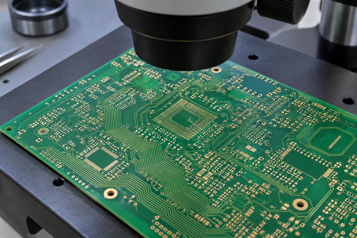
How do the two process flows form copper traces?
The main difference is where the final copper thickness comes from and how much unwanted copper must be removed. The sequences below explain the principle; actual multilayer and outer-layer flows include additional operations and variants.
Subtractive route: protect the pattern and remove the rest
- Prepare a copper-bearing surface for the imaging process.
- Form the protective pattern that defines the copper to retain.
- Etch the unwanted copper and remove the temporary process resist as required by the route.
- Inspect the resulting pattern against the finished requirements.
Etching can affect the sides as well as the exposed face of a copper feature. The engineering task is to control the final conductor geometry while fully clearing spaces. Read the PCB etch-factor and undercut explanation when discussing artwork compensation with a fabricator. Do not add a guessed compensation value to already approved production data.
Semi-additive route: build the pattern before clearing the thin base
- Establish the thin conductive base on the specified dielectric or foil-based structure.
- Image and develop resist openings where copper is to be built.
- Plate copper in those openings to form the intended conductors.
- Strip the temporary resist and remove the exposed conductive base between conductors.
- Verify dimensions, separation and the interconnections required by the construction.
“Semi-additive” therefore does not mean “no etching.” Removing the remaining conductive base is necessary to separate the circuits. The process avoids having to remove the full final conductor thickness from every space, but it still needs control of the final copper geometry.
NISSHA’s SAP development page illustrates the motivation for selective copper build-up: narrow conductors, adjustable copper thickness and a more rectangular profile in its specific film-patterning application. That example explains a mechanism; it is not a promise of identical geometry for every PCB material or factory. Source: NISSHA SAP overview.
Which DFM rules must be requalified?
Requalify the rules that define the finished copper and its connection to the stackup. Do not take a subtractive rule set, reduce only the minimum trace width, and assume the rest remains valid.
| Rule area | Question for the fabricator | Required design decision |
|---|---|---|
| Line width and spacing | Which dimensions are CAD targets and which are accepted finished limits? | Use the agreed rule set for each affected layer and feature type. |
| Copper thickness and profile | What finished range and cross-sectional assumptions apply? | Check current, resistance and impedance with the agreed geometry. |
| Dielectric and adhesion | Which exact material construction is qualified for this process? | Lock material identity and control proposed substitutions. |
| Vias and capture pads | What layer spans, diameters, pads and connection structures are approved? | Route within the supported interconnect architecture, not just the line/space limit. |
| Pattern distribution | Are there density or balancing requirements for this layout? | Agree any nonfunctional copper additions before release. |
| Inspection and coupons | How will the tightest and highest-risk features be measured? | Reserve any required coupon area and define acceptance evidence. |
A capability statement such as “fine-line process available” leaves too much unresolved. Ask whether a quoted dimension applies to isolated lines, repeated dense patterns, the selected copper thickness, a test vehicle or routine production. These are different claims.
Atotech’s amSAP technical paper describes why a thin surface deposit alone is not enough: deposit uniformity, removal of residues and microvia coverage must be controlled together. A process adjustment that helps clear narrow spaces can create a different reliability risk if coverage is inadequate. This is evidence for reviewing the process as a system, not for copying a single minimum dimension. Source: Atotech amSAP technical paper.
For controlled impedance, give the fabricator the target and applicable tolerance, then agree the stackup and finished geometry used for modeling. A more rectangular-looking conductor is not by itself a verified impedance result. Likewise, a narrow route that solves component escape still needs an electrical review for its intended load and signal behavior.
When does finer routing justify a different process?
Consider a different process when an identified routing bottleneck cannot be solved acceptably within a qualified conventional construction. Compare it with layout changes, a different component package and alternative layer arrangements before committing to a process transition.
A simple routing-channel example
For N parallel traces of width w, separated by spaces s, the geometric width of the trace group is Nw + (N – 1)s. This excludes clearance to obstacles on either side.
For four traces at 75 µm width and 75 µm spacing, the group occupies 4 × 75 + 3 × 75 = 525 µm. At an illustrative 40/40 µm, it occupies 4 × 40 + 3 × 40 = 280 µm. The difference is 245 µm before outside clearances.
These are hypothetical geometry values, not PCBtry process limits and not a boundary between subtractive and semi-additive manufacturing. The example helps locate a routing opportunity; it does not establish manufacturability. Pads, vias, obstacle clearances, return paths and electrical requirements may still control the available channel.
Now ask what the smaller channel actually saves. Does it remove a routing layer, avoid a larger board or enable a required component package? If it only makes an already workable layout slightly tidier, the transition may not justify qualification effort or a narrower supplier choice.
Compare quotations on the same drawings, quantity, materials, test scope and acceptance requirements. Include engineering setup, qualification builds, anticipated yield assumptions disclosed by the supplier and the cost of future changes. Do not assume that less copper removed automatically means a cheaper finished board.
Also identify which layers need the finer process. A possible mixed construction must be reviewed and quoted explicitly; it is not something to infer from the fact that a supplier offers several process families.
What evidence should a fabrication review produce?
It should produce an agreed construction, a controlled design-rule set and a plan to verify the actual product. A technology brochure is useful background, but it does not replace those release documents.
| Risk being reviewed | Evidence to request | What it does not prove by itself |
|---|---|---|
| Finished fine-line geometry | Defined measurement method, location and accepted width/space/profile limits | One attractive microscope image does not establish production variation. |
| Interconnect reliability | Applicable qualification plan and results for a representative construction | A room-temperature continuity pass does not prove service-life reliability. |
| Electrical performance | Agreed stackup, simulation inputs and required verification | A process name does not guarantee impedance or insertion loss. |
| Production repeatability | Lot/panel sampling plan and relevant capability evidence | A prototype result is not automatically a mass-production guarantee. |
| Change control | Approved material/process revisions and notification requirements | A purchase order with only a generic material name leaves substitutions ambiguous. |
Bring this discussion into the DFM review before fabrication. If a dimension or reliability requirement cannot be confirmed, keep that item open and assign an owner instead of treating a quotation as technical approval.
Prepare these inputs for a process comparison:
- Board outline, layer count and proposed stackup.
- The exact layers and areas that need fine routing.
- Minimum intended width/space and finished copper requirements.
- Component escape geometry, via structure and land-pattern constraints.
- Electrical targets, environment and required reliability verification.
- Prototype and production quantities, release date and change-control requirements.
Keep the approved response with the fabrication revision. When a component, material or copper requirement changes, revisit the affected rules rather than assuming the previous approval still covers the new construction.
Frequently asked questions
Is SAP the same as mSAP?
No. They share selective copper build-up, but the starting conductive structure differs. Suppliers may also offer proprietary variants. Ask for the actual construction and process definition rather than relying only on the abbreviation.
Does semi-additive processing eliminate etching?
No. The exposed conductive base between the plated features still has to be removed. Its removal is part of achieving electrical separation and the required final geometry.
Is LDI a competing process to SAP?
Not in the same classification. Laser direct imaging is an imaging method; SAP describes a copper-patterning route. Discuss imaging capability as one part of the overall process rather than treating the names as mutually exclusive alternatives.
Is every HDI board made using a semi-additive process?
No. HDI describes an interconnect construction category, not a single copper-patterning route. Establish how the proposed board will actually be built and which rules apply.
Can I use a published minimum line width as my design rule?
Only after the supplier confirms it for your construction and acceptance requirements. A research result, isolated test feature or marketing headline may not describe repeatable production on your board.
Will finer traces always improve signal integrity?
No. Signal behavior depends on the whole interconnect, including geometry, dielectric, reference path and transitions. A density improvement is not automatically an electrical improvement. Recheck the relevant model and verification plan.
Can the same files be sent to either process?
The design intent may be transferable, but a process change can require new rules, stackup assumptions and fabrication notes. Obtain a fresh review before release; do not silently switch suppliers or processes.
Does PCBtry offer the exact semi-additive construction I need?
That needs project-specific confirmation. Send the proposed construction and fine-line requirements and ask which manufacturing route, materials and verification can be supported. This comparison is not a capability certification.
To review the available route for your design, contact PCBtry with the stackup, fabrication data and marked routing bottlenecks. Ask for written confirmation of the supported construction and finished limits before finalizing the layout.



0 Comments