
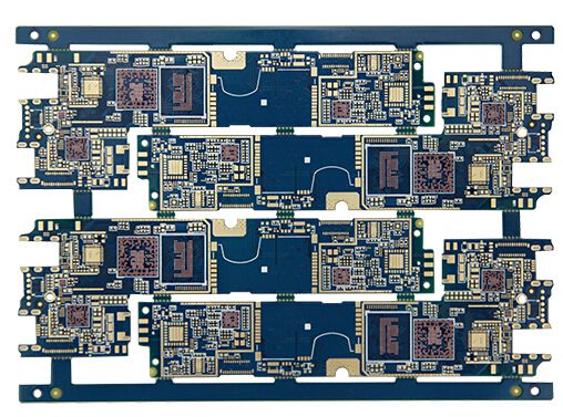
HDI PCB, its full name is High-Density Interconnect Printed Circuit Board, has become one of the most sought-after solutions for compact and high-performance electronics. These boards are designed to pack more components into a smaller footprint without compromising signal integrity. You can find HDI PCBs inside your smartphones, tablets, laptops, medical devices, and even in military systems.
In this guide, we’ll walk you through what HDI PCBs are, how they work, the advantages they bring, and what to consider when designing or fabricating one.
What Is HDI PCB?
HDI PCB refers to a PCB with a higher wiring density per unit area than traditional boards. This is achieved using microvias, blind and buried vias, fine trace widths, and dense component placement.
Compared to regular PCBs, HDI PCBs are more advanced and are often used in applications where space and performance matter the most. These include smartphones, smartwatches, medical implants, advanced automotive control systems, and aerospace communication units.
So, when someone asks for the HDI PCB definition, it refers to a circuit board designed to allow for higher electrical performance in a smaller size, with tighter spacing and more layers of interconnection.
HDI PCB Stackup
The HDI PCB stackup refers to how the layers of copper and insulation are arranged in a multilayer board. An optimized stackup improves signal integrity, reduces electromagnetic interference (EMI), and helps with thermal distribution.
Common Stackup Formats:
- 1+4+1 Stackup: One HDI layer on both sides of a four-layer core. Compact and cost-effective.
- 2+6+2 Stackup: Two HDI layers per side, great for complex routing and BGA designs.
- Any-Layer Stackup: All layers use microvias for full interconnection flexibility.
When designing your stackup, always consider impedance control, grounding, and signal routing paths. A well-balanced HDI stackup reduces noise and improves overall board performance.
HDI PCB Types
HDI PCBs are available in several configurations based on how their vias (vertical interconnects between layers) are arranged. Here are the main types of HDI boards:
1. 1+N+1 HDI PCB
This is the most basic type of HDI multilayer PCB. It has one layer on the top and one on the bottom, surrounding a core (N). “N” refers to the core board with standard through-hole layers. “1” indicates an additional HDI layer added to both sides. For example, 1+4+1 means a 4-layer core board with one HDI layer on top and bottom. This requires 2 press cycles. It uses laser-drilled microvias to connect the layers. This design is ideal for moderate-density applications like consumer electronics.
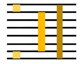
2. 2+N+2 HDI PCB
This board adds two HDI layers to each side of the core board. For example, 2+4+2 means a 4-layer core with two HDI layers added to each side. This structure requires three lamination cycles. It’s often used in mid- to high-complexity applications. It supports stacked microvias, via-in-pad, and staggered vias.
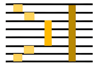
3. 3+N+3 and Beyond
These are used for advanced computing or communication systems. The more HDI layers you add, the more routing options you get—but also, the cost and fabrication complexity rise. For example, 3 +8+3 requires four lamination cycles to complete. First, laminate 3–6 layers, then another 2–4 layers, and finally 1–2 outer layers. A total of three press cycles are involved.
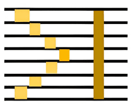
4. Any Layer HDI PCB
In this structure, microvias can connect any layer to any other layer. It uses laser drilling and stacked via techniques to build the vertical interconnections. Common in high-end smartphones and military systems, this type allows signal transmission across any two layers with minimal distance.
What Defines HDI PCB?
An HDI PCB is defined by the presence of at least one of the following:
- Microvias: Small laser-drilled vias, typically less than 150µm in diameter.
- Blind/Buried Vias: These don’t pass through the whole board. They connect internal or surface layers.
- Fine Line Traces and Spaces: Traces can be as narrow as 50µm.
- High Pad Density: More component pads packed per square inch.
When a PCB integrates two or more of the above, it qualifies as an HDI board.
Advantages of Using HDI PCB
1. Support more components in a smaller footprint, so smaller size, more functionality.
2. Shorter signal paths and controlled impedance improve signal integrity
3. Due to its high wiring density, an HDI PCB can often achieve the same circuit complexity in fewer layers than a traditional board.
4. Tight layout control and better material usage help HDI PCBs manage heat more effectively, reducing hotspots.
5. Fine-pitch BGAs, flip-chip packages, and stacked die components are available to mount while without increasing board size.
What Is the Difference Between HDI PCB and Normal PCB?
The difference between an HDI PCB and a normal PCB goes far beyond just size or density. They differ in materials, design rules, performance, and manufacturing complexity. Here’s a more comprehensive comparison:
| Feature | Normal PCB | HDI PCB |
| Via Types | Typically uses only through-hole vias, which span from the top to the bottom layer. | Uses microvias, blind vias, buried vias, and stacked vias for high-density interconnects. |
| Trace Width & Spacing | Usually ≥ 100µm. | Can be < 75µm, even down to 40µm in advanced designs. |
| Layer Count | Often 2 to 10 layers, depending on the product. | Commonly 8 to 20+ layers, with complex routing across multiple HDI layers. |
| Board Thickness | Standard thicknesses range from 0.8mm to 2.4mm. | Can be much thinner (<0.6mm) to fit compact devices. |
| Pad Density | Lower component pad density, more open routing space. | High pad density for mounting fine-pitch BGAs, QFNs, and other dense components. |
| Signal Integrity | Suffers at high frequencies due to longer trace lengths and poor impedance control. | Improved signal performance, low crosstalk, and better impedance control. |
| Material Type | General-purpose FR-4 or mid-Tg materials. | Uses high-Tg, low-loss, and sometimes RF-compatible materials. |
| Manufacturing Process | Uses standard drilling, plating, and etching. | Involves laser drilling, sequential lamination, and advanced imaging techniques. |
| Surface Finish | HASL, OSP, Immersion Tin common. | Requires flat finishes like ENIG to accommodate fine-pitch components. |
| Design Complexity | Less restricted in terms of design spacing. Easier to lay out. | Highly constrained layout. Requires precise spacing, routing, and layer planning. |
| Cost | Lower due to simpler process and common materials. | Higher due to advanced processing, material costs, and inspection requirements. |
| Application Area | Suitable for consumer electronics, industrial controls, and simple devices. | Essential for smartphones, tablets, aerospace, medical implants, high-speed devices. |
| Design Software Requirements | Basic PCB layout tools sufficient. | Needs tools with HDI support (e.g., Altium Designer, Cadence Allegro). |
| Heat Dissipation | Less efficient thermal pathways. | Better heat distribution with the use of thermal vias and denser copper planes. |
| Testing Requirements | Standard test methods (flying probe, visual inspection). | Requires advanced testing methods like X-ray inspection for buried structures. |
| Repairability | Easier to rework or modify during prototyping. | Difficult to rework due to smaller features and hidden interconnections. |
So in a conclusion, if your project involves high-speed signals, compact dimensions, or complex multi-layer interconnects, then an HDI PCB is the right choice. But for simpler, low-cost applications, a standard PCB may be more suitable.
Key Considerations of HDI PCB Design Guide
Designing an HDI PCB involves more than just shrinking trace widths or adding more layers. It requires a careful balance of electrical, mechanical, and manufacturing considerations to ensure performance, reliability, and cost-efficiency. Here’s a complete design guide to help you through the process.
1. Decide the Application Requirements
Before starting the design, define the performance targets of your product:
- Is the board for high-speed data transfer (e.g., USB 3.1, DDR4, PCIe)?
- Does it need to fit into a compact enclosure like a smartphone?
- Are there thermal or power delivery challenges?
- What is the expected layer count or board size?
Understanding the end-use environment helps determine the need for HDI and its complexity (e.g., 1+N+1 vs. 3+N+3 vs. Any-Layer HDI).
2. Choose the Right Stackup and Via Strategy
The stackup determines how layers are arranged and how signals are routed. Common stackups include:
- 1+N+1: Basic, for moderate-density products.
- 2+N+2 or 3+N+3: For complex BGA or flip-chip designs.
- Any-Layer HDI: For highly compact products like flagship smartphones.
Via Types:
- Microvia – laser-drilled; used for short, high-density connections.
- Blind via – connects outer layers to inner layers.
- Buried via – connects internal layers without appearing on the outer layer.
- Stacked via – vertical stack of microvias connecting multiple layers.
Use staggered vias when possible to enhance structural strength and yield. Stacked vias, while more compact, are harder to manufacture and costlier.
3. Design With HDI Rules and Constraints
HDI boards follow stricter DRC (Design Rule Check) constraints than traditional PCBs. Set your CAD software rules accordingly below or confirm with your PCB manufacturer:
| Design Element | HDI Typical Values |
| Minimum trace width | 50–75 µm |
| Minimum trace spacing | 50–75 µm |
| Microvia diameter | 75–100 µm |
| Pad size | ~0.3 mm for microvias |
| Aspect ratio | Typically < 1:1 for microvias |
4. Routing High-Speed Signals
HDI PCBs are ideal for high-speed digital and RF signals, but routing must be optimized:
- Use short, direct traces to reduce signal degradation.
- Route differential pairs (e.g., USB, HDMI, PCIe) with tight length matching and consistent spacing.
- Ensure impedance control using well-defined trace width and spacing relative to the dielectric thickness.
- Use solid reference planes to provide consistent return paths and reduce EMI.
- Avoid 90° bends in signal traces; use 45° bends or curved traces instead.
Why Choose Thindry as Your HDI PCB Manufacturer?
At Thindry circuits, we specialize in HDI PCB fabrication and multilayer designs for demanding industries like aerospace, automotive, and consumer electronics.
Here’s why engineers and designers trust us:
- Capabilities for 1+N+1 to Any-Layer HDI PCB stackups
- Precise laser microvia drilling and sequential lamination
- Fast prototyping and high-volume production
- Professional PCB engineer for one-to-one service
- PCB design, PCB layout, HDI PCB manufacturing
- Fast delivery with high quality
Whether you need a simple 1+4+1 layout or a complex 3+N+3 stackup, our engineers are here to support you from design to delivery.
FAQs
1. What does HDI mean in PCB manufacturing?
It means High-Density Interconnect. HDI boards have finer lines, smaller vias, and denser pad placement compared to traditional PCBs.
2. What’s the smallest via size used in HDI boards?
Microvias typically have diameters as small as 75–100µm, far smaller than standard through-holes.
3. Can I prototype HDI PCBs affordably?
Yes. Best Technology offers fast-turn HDI prototyping services with flexible pricing.
4. How many layers can HDI PCBs support?
They can go up to 20+ layers depending on the application and manufacturer capabilities.
5. What surface finishes are used in HDI PCBs?
ENIG is the most common due to its flatness and reliability, but OSP, immersion silver, and gold plating are also used.


0 Comments