Blog
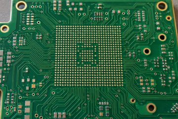
HDI PCB Design Guide: Read Stackups and Check BGA Escape
Learn to read HDI stackups, map microvia layer pairs and check BGA escape geometry, with worked examples and a practical pre-layout checklist.



Learn to read HDI stackups, map microvia layer pairs and check BGA escape geometry, with worked examples and a practical pre-layout checklist.
If you have any enquiry about quotation or cooperation, please feel free to email us at sales@pcbtry.com or use the following enquiry form. Oursales representative will contact you within 24 hours. Thank you for your interest in our products.