




An HDI PCB (high-density interconnect printed circuit board) uses small interconnections and fine routing features to fit more connections into a given area. For a designer, the useful question is not whether HDI is more advanced. It is whether the proposed pads, traces and layer-to-layer connections let the circuit be routed and manufactured reliably.
This guide works through that question in order: read the stackup, calculate the space available between pads, trace a connection through the layers, and identify what still needs the fabricator’s approval. The numerical examples are hypothetical teaching examples, not PCBtry manufacturing limits.
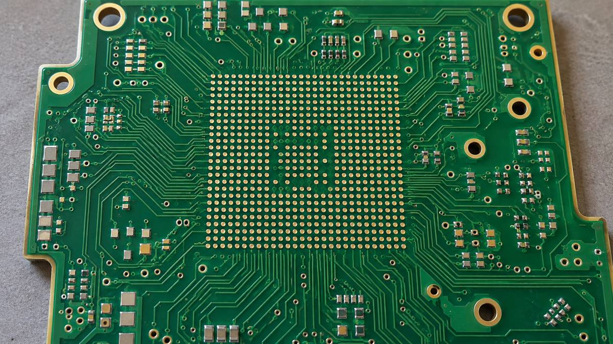
What changes when a PCB uses HDI?
HDI changes how much routing space a connection occupies and which layers it can reach. Smaller pads and short microvia connections can make room for signals that would be difficult to escape using larger through-vias.
A via is a conductive connection between copper layers. Imagine trying to route a signal away from a pad in the middle of a ball grid array (BGA). On the surface, neighboring pads block the route. A suitable via can move that signal to another layer, where there may be room to continue.
However, the hole must connect to the intended copper. A plated through-via spans the board, but it does not automatically connect electrically to every layer: unwanted connections are prevented with copper clearance around it. A blind via reaches an internal layer from a surface; a buried via connects internal layers. These terms describe accessibility, not one universal hole size.
Microvias are short, small interconnections commonly formed with lasers. The hole depth, opening, landing pad and manufacturing process must work together. A via-in-pad describes where a via is placed; it is not a synonym for microvia. See the separate PCB via types guide for the wider comparison.
Do not identify HDI solely by board thickness, layer count, FR-4 material or a gold-colored finish. Equally, the HDI label does not guarantee lower loss, better cooling or lower cost. Those outcomes still depend on the actual circuit, materials and geometry.
How do you read 1+N+1 and 2+N+2 stackups?
Read these expressions as a description of the build-up layers around an inner structure, then use the drawing to identify the permitted connections. The shorthand alone is not a drill map.
| Notation | Plain-language reading | Example copper-layer count | What still needs a drawing |
|---|---|---|---|
| 1+N+1 | One build-up copper layer on each side of an N-layer inner structure | 1+4+1 = 6 layers | Outer microvia pairs, internal vias and through-vias |
| 2+N+2 | Two build-up copper layers on each side | 2+4+2 = 8 layers | Whether successive microvias are stacked or offset; their approved landing pads |
| Any-layer / ELIC | A construction offering interconnection through successive microvia layers | Read the actual stackup | The complete chain between the start and destination layers |
Here is a hypothetical six-layer 1+4+1 board, numbered from top to bottom. L1 and L6 are the outer build-up layers. L2 through L5 form the inner four-layer structure. If the drawing specifies L1-L2 and L6-L5 microvias, an L1-L2 microvia reaches L2, not L3.
To continue from L2 to L3, you need an additional approved connection. It might be an internal via or another permitted structure, depending on the build. Drawing a line to L3 in CAD does not create a manufacturing route that the stackup lacks.
Likewise, “2+4+2” does not by itself tell you whether the microvias are stacked or staggered. Stacked microvias sit above one another; staggered microvias are laterally offset, with copper joining them on the intermediate layer. Ask for both a cross-section and a layer-pair drill table.
Do not convert the notation directly into a guaranteed number of press cycles. The inner structure and fabrication sequence also matter. Altium’s HDI design guidance explains why sequential build-up and via formation must be considered together. For the factory sequence rather than the drawing-reading task, use the HDI PCB manufacturing process guide.
Can the BGA pads and escape traces actually fit?
Check the copper pad diameter and required clearances, not just the BGA pitch. Pitch is the distance from the center of one pad to the center of the next. The usable gap is smaller because the pads occupy part of it.
A one-trace screening calculation
For a straight trace passing between two equal circular copper pads, define pitch P, pad diameter D, trace width W, and required trace-to-pad clearance C. Use the same units throughout:
Available gap = P − D
Required gap for one trace = W + 2C
Geometric margin = (P − D) − (W + 2C)
| Hypothetical input | Example A | Example B |
|---|---|---|
| Pitch P | 0.50 mm | 0.40 mm |
| Copper pad diameter D | 0.25 mm | 0.25 mm |
| Trace width W | 0.075 mm | 0.075 mm |
| Clearance C on each side | 0.075 mm | 0.075 mm |
| Available gap P − D | 0.250 mm | 0.150 mm |
| Required gap W + 2C | 0.225 mm | 0.225 mm |
| Nominal geometric margin | +0.025 mm | −0.075 mm |
Example A passes this simple geometric screen. Example B does not: the proposed line and its two clearances require more space than the pads leave. The same line rule can therefore work at one pitch and fail at another.
A positive margin is not manufacturing approval. Confirm whether your design rules refer to nominal artwork or finished copper, how tolerances are covered, and whether the solder mask and assembly requirements are satisfied. Do not subtract the solder-ball diameter when the copper land diameter is the feature limiting the route.
When the calculation fails
- Verify the package manufacturer’s recommended land pattern and the intended assembly process.
- Check whether a different approved escape route is available. The next row of pads or vias may block a locally valid channel.
- Ask the fabricator whether narrower lines and spaces are practical for the chosen copper and layer.
- Evaluate an approved via-in-pad or near-pad microvia route, a different stackup, or a different package.
Do not shrink a pad just to make the equation pass. The pad also has an assembly job. And do not treat this one-trace check as a full BGA fanout calculation: ball assignments, multiple rows, power connections, via lands and routing direction can change the result.
How do you check a route through the layers?
Follow one difficult signal from its component pad to its destination, recording every layer change and reference plane. This exposes impossible connections before they spread across the layout.
- Start with a specific pad. Record its net, copper land size and available escape direction.
- Name the first layer transition. For example, L1-L2, rather than simply “microvia.” Check the capture pad, target pad and neighboring clearances.
- Inspect the landing layer. A connection arriving on L2 is useful only if there is an approved route onward. Do not assume a ground plane is a free signal-routing layer.
- Follow each remaining transition. Identify the actual via structure used to reach the destination. Check both physical clearance and electrical connectivity.
- Check the return path. For high-speed signals, review the reference plane and return-current path at transitions with the interface requirements in mind.
On the hypothetical six-layer board, suppose L2 is intended as an uninterrupted ground reference. Moving an L1 signal to L2 and then drawing a long trace across that plane may solve one escape problem while disrupting other signals’ return paths. That is a reason to revisit the stackup or escape scheme, not to silently turn a plane into an arbitrary routing layer.
The check is complete only when the net reaches its destination using manufacturable connections. “The pad fits” and “the via exists” are intermediate checks, not the finished answer.
Which design rules must the fabricator confirm?
Obtain rules for the proposed build, not a disconnected list of the supplier’s smallest advertised features. Minimum hole size, line width and copper thickness may not all be available together.
| Ask for | Why it changes the layout | Record before routing |
|---|---|---|
| Permitted via layer pairs | Determines which layers a signal can reach | Cross-section and drill table |
| Microvia depth and diameter definition | Controls drilling and plating feasibility | Agreed opening, depth and aspect-ratio limit |
| Capture and target pad dimensions | Provides registration allowance and consumes routing space | Pad sizes and copper clearances |
| Line/space for each copper condition | Fine features depend on copper and processing | Layer-specific approved rules |
| Via filling and surface requirements | Affects component-pad flatness and assembly | Fill, cap and permitted surface condition where applicable |
| Dielectric and finished copper | Changes impedance, thickness and thermal behavior | Approved material and stackup tolerances |
| Qualification and acceptance evidence | Checks whether the proposed structure meets the application | Agreed test method, conditions and acceptance criteria |
For example, a hypothetical 0.075 mm-deep hole with a 0.100 mm specified diameter gives a depth-to-diameter ratio of 0.75. That arithmetic is straightforward; deciding which opening definition applies to a tapered hole and whether the structure is qualified is a fabricator question. A ratio alone cannot approve the via.
NCAB’s HDI technical guidance connects land dimensions and via geometry with manufacturing risks. Treat its recommendations as supplier guidance, not as universal limits or proof of another factory’s capabilities.

What proves an HDI design is ready for fabrication?
Readiness requires a consistent fabrication package, resolved design-rule issues and an agreed validation plan. A clean CAD check is useful, but it cannot prove that every internal interface will survive assembly and service.
IPC has reported microvia failures that escaped traditional acceptance inspections and appeared during later assembly or service. Its microvia reliability warning is a reason to discuss appropriate performance-based testing, especially for stacked structures. It is not evidence that all stacked microvias fail.
Room-temperature continuity, a surface photograph or X-ray inspection alone cannot establish long-term microvia-interface reliability. Agree on suitable coupons, thermal exposure, electrical monitoring and acceptance criteria for the product and construction. Use the applicable current standard and customer specification, not an isolated number copied from a blog.
Save this pre-layout and release checklist:
- The BGA land pattern matches the selected package and assembly requirements.
- The hardest escape routes have been checked, not just the outermost pad row.
- Each via has an explicit start layer, end layer and approved geometry.
- Signal routing does not silently consume required reference-plane areas.
- The stackup, copper, material and impedance requirements agree with one another.
- Via-in-pad filling and surface requirements are explicitly stated.
- CAD rules match the fabricator’s approved build rules.
- Unresolved exceptions are documented and answered before release.
- The test plan distinguishes initial connectivity from reliability validation.
- Fabrication data, drill information, stackup and drawings share the same revision.
For an early review, send the package datasheet or land-pattern reference, preliminary layout, proposed stackup, via table, board dimensions, thickness constraints and electrical requirements. For fabrication, add the agreed production data format, drill files and fabrication drawing. BOM and component-placement files belong in the package when assembly is also requested.
HDI design questions that need careful answers
Does an HDI PCB have to use a special laminate?
No single material name defines HDI. Material selection depends on electrical, thermal and processing requirements. Specify the required properties and an agreed material, rather than assuming all FR-4 grades behave alike.
Is ENIG mandatory for HDI?
No. Surface finish is a separate decision influenced by component pitch, assembly, storage and reliability requirements. Confirm the finish for the actual design instead of choosing it solely because the board uses microvias.
Does a 0.4 mm BGA always require the same via structure?
No. Pitch alone leaves out copper pad size, ball assignments, escape directions and manufacturing rules. Evaluate the particular land pattern and complete routing task before choosing a structure.
Can I copy another board’s impedance trace width?
Not safely without its stackup context. Dielectric thickness and properties, finished copper, nearby reference conductors and manufacturing tolerances matter. Recalculate and confirm the geometry for your board.
Should every via on the board be a microvia?
No. Different connections can use different approved structures. A through-via may remain suitable away from a dense package. Use the structure needed for the connection rather than making every feature equally complex.
Can a supplier change the layer arrangement after layout?
A proposed change needs engineering review. It may affect layer access, impedance, return paths and routing assumptions. Recheck the affected nets and issue matching revised files before fabrication.
Does passing DRC mean the board will work?
No. DRC checks the rules that were configured. It does not establish that those rules match fabrication capability or that the circuit meets its electrical and reliability requirements.
Can HDI lower the finished product cost?
It can in some designs, but not automatically. Compare achievable board size, layer count, fabrication complexity, assembly and qualification for equivalent requirements. A fixed percentage saving is not a substitute for comparable quotations.
Need a review of your proposed layer connections? Send your stackup, BGA information, via table and layout through PCBtry’s contact page. Ask for the permitted layer pairs and design rules for that specific build before committing to the layout. The HDI PCB service page provides the relevant manufacturing contact route; feasibility remains subject to review of your files.



0 Comments