




A PCB solderability test checks whether the intended metal surfaces can be wetted by solder under defined conditions. It does not prove that every joint will assemble correctly. When solder beads up, first separate a surface-finish problem from inadequate heat transfer, an unsuitable flux system, or a physically missing pad. That distinction prevents an expensive board lot from being rejected for the wrong reason.
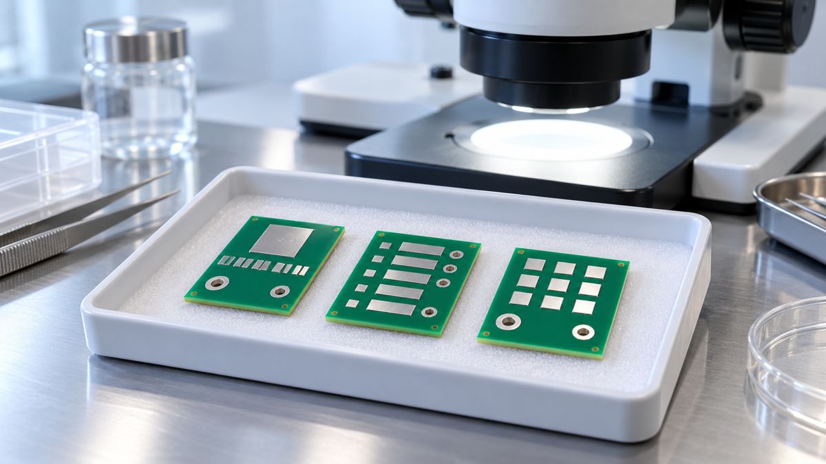
What does a PCB solderability test actually prove?
Think of solderability as a surface’s willingness to form a soldered connection under a controlled test. Electrical continuity answers a different question: whether a conducting path exists. A board can pass an electrical test yet have a surface that is difficult to solder.
The public scope of IPC J-STD-003D covers printed-board conductors, attachment lands and plated-through holes. It explicitly separates finish wettability from successful assembly processing. Specify the applicable standard revision and method with the laboratory; this guide does not reproduce the full standard or supply universal acceptance limits.
For a practical example, a coupon may wet in a controlled bath while a large ground-connected pad fails during hand soldering. That result directs attention toward the assembly setup, but does not automatically clear every feature on the production board. Coupon geometry, panel location and subsequent handling still matter. Use solderability evidence alongside the broader PCB testing and release plan.
When should you test a bare PCB?
Consider a defined test when an incoming lot shows unexplained wetting failures, stored boards are being released after uncertain handling, a surface finish or supplier changes, or a customer specification requires it. Testing is most useful when it answers a recorded question, such as whether an unopened retained sample behaves differently from material exposed on the production floor.
Keep representative as-received boards or coupons untouched. Record the lot, finish, manufacturing date, package-opening date and storage history. Photograph the suspect features before cleaning, baking, scraping or reworking them. Those treatments may change the very surface you need to investigate.
Agree the sampling plan and any preconditioning before sending samples. Do not quietly substitute an accelerated-aged specimen for an as-received specimen, or treat one successful sample as proof that an entire lot is uniform. If no panel coupon remains, ask the laboratory which production features it can test and what that limits.
Dip-and-look vs wetting balance: which test should you request?
Choose by the evidence needed, not by the sophistication of the instrument. The first approach emphasizes the condition after solder contact; the second records a response over time. Neither is a substitute for an agreed acceptance procedure.
| Approach | Useful output | Best question to ask | Important limitation |
|---|---|---|---|
| Dip-and-look | Inspection of coverage and wetting appearance after controlled solder exposure | Does the specified surface satisfy the agreed visual criteria? | Photography, inspection method and relevant feature definition must be consistent. |
| Wetting balance | Force-versus-time curve during immersion | Does wetting behavior differ between matched specimens? | Geometry, immersion and alloy affect the result; raw curves from unlike specimens are not interchangeable. |
| Assembly process trial | Joint results under the intended paste, flux, thermal profile and equipment | Can this board be assembled using the intended process? | Several variables interact; failure alone does not identify the board finish as the cause. |
Fraunhofer ISIT explains wetting-balance measurement as a load-cell observation during immersion. The resulting force-time trace supports comparison of wetting delay, force and progression. Request the curve and specimen details, not only a label saying “pass.” Before interpreting the trace, confirm the instrument’s sign convention and the laboratory’s evaluation method.
Kester 951 flux parameters: what must stay controlled?
Flux is not an invisible background variable. The following example shows why a product name and controlled condition belong in a process record. Kester 951 is a commercial wave-soldering flux, not an automatic substitute for the flux prescribed by a solderability-test method.
| 951 parameter | Published value or condition | How to use it |
|---|---|---|
| Specific gravity | 0.814 at 25°C, Anton Paar DMA | Compare measurements at the stated temperature; no production tolerance is given here. |
| Solids | 2.0%, theoretical | Do not confuse liquid volume with deposited solid mass. |
| Acid number | 14.3 mg KOH/g flux, typical | A characterization value, not a universal acceptance band. |
| Recommended deposition | 120–240 µg solids/cm² | Application guidance for this product, not for every flux. |
| Preheat guidance | 93–115°C measured on the component side | Board temperature is not the heater setting or solder-bath temperature. |
Source: Kester 951 technical data sheet, issued 13 May 2021. Values apply to this named flux. They are not PCB material ratings, maximum component temperatures, or a guaranteed process window for your assembly. Obtain supplier control limits and follow the SDS. The product is flammable; use appropriate handling and ventilation.
If a comparison changes the flux and the board lot together, a better result cannot isolate which change helped. For a controlled investigation, keep the specified flux system constant while comparing lots; evaluate a production-flux change as a separate, documented experiment.
Why does solder fail to wet a PCB pad?
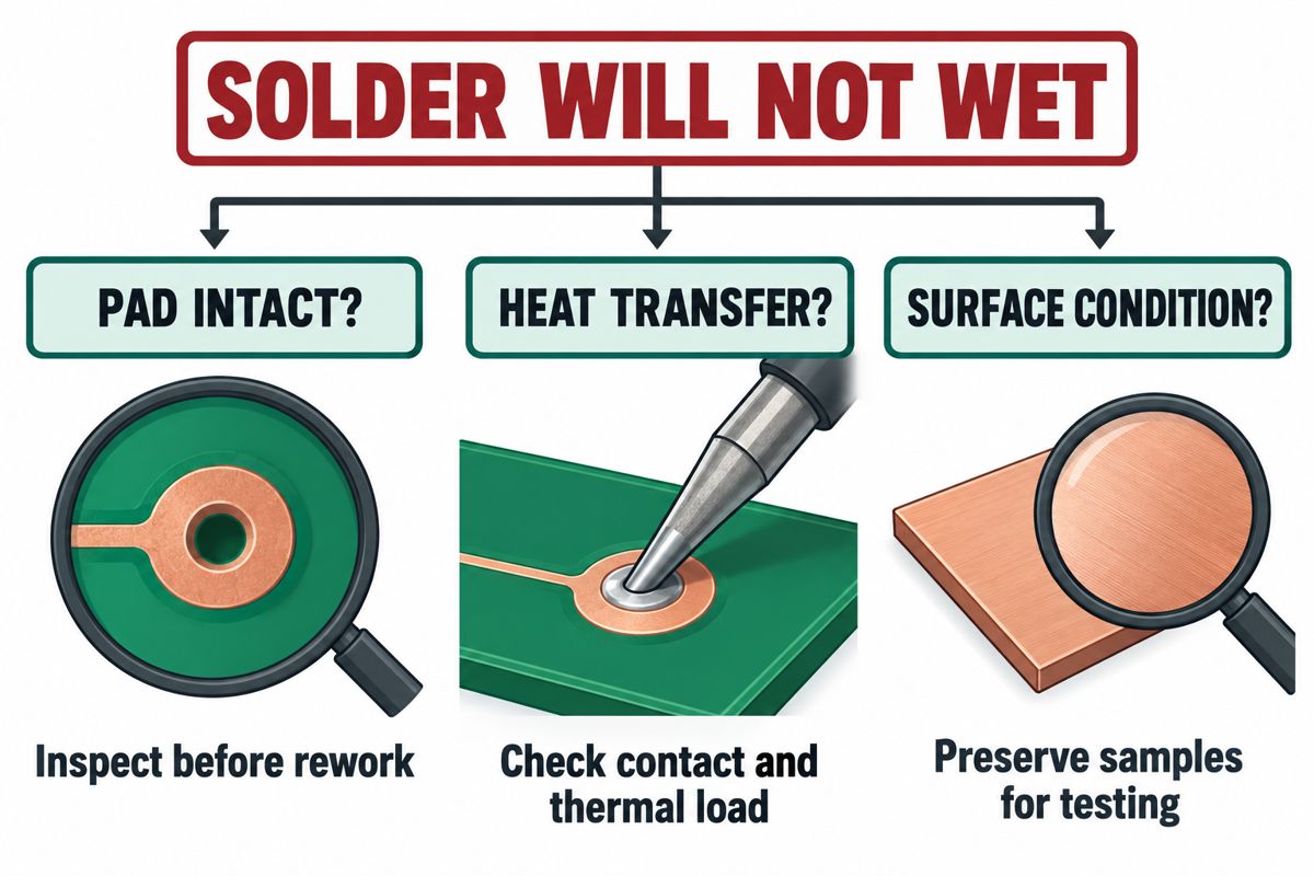
Start with a microscope or clear magnified photographs. Is there an intact metal pad, or exposed laminate where a pad used to be? Is the intended contact actually a solderable land rather than a coated switch contact? Repeated heating cannot restore missing metal.
Next inspect the thermal path. Solder melting on the iron proves the tip can melt solder; it does not prove the pad reached the required condition. A poor contact area or a large connected copper plane can leave the joint cold while the tip is hot. Check tip condition, contact, thermal capacity and the approved process before increasing temperature.
Finally investigate surface and consumable history: handling contamination, finish degradation, flux identity, age and application. Avoid assigning a specific chemical failure such as “black pad” from a dark photograph alone. Preserve failed and unaffected specimens for the appropriate analysis.
What should a solderability test report include?
Use this matrix before authorizing a test. A certificate without traceability or conditions is difficult to compare with a later failure investigation.
| Record | What to request | Hold the conclusion when… |
|---|---|---|
| Sample identity | Lot, finish, panel position or board feature, sample count | The sample cannot be tied to the suspect lot. |
| Conditioning | As-received status, storage, aging, cleaning or baking history | A treated sample is presented as untouched material. |
| Method | Standard revision, test method, customer exceptions | Only “IPC tested” is written. |
| Controlled inputs | Alloy, flux, temperature, contact time and specimen geometry as applicable | Compared results used different uncontrolled conditions. |
| Results | Feature-level photographs or curves, observations and acceptance clause | A pass/fail word has no supporting measurement or inspection record. |
| Disposition | Responsible reviewer, lot decision, retest scope and corrective action | A small sample is used to claim unrestricted lot approval. |
Save the matrix with your purchase specification. The useful deliverable is a decision you can defend later, not simply another inspection certificate.
How do you investigate a failed PCB lot?
- Contain and identify. Separate suspect stock and record affected features, quantities and process steps. Keep untreated samples.
- State the hypothesis. Write whether you suspect the finish, storage exposure, thermal access or consumables. List what would disprove it.
- Agree the test. Define representative samples, method, conditions and acceptance authority with the supplier or laboratory.
- Compare like with like. Include an appropriate reference and change one explanatory variable at a time where feasible. Record deviations instead of hiding them.
- Verify the intended assembly. A favorable surface result still needs a suitable production process. Review joint quality using the applicable assembly requirements.
- Release with evidence. Record the scope of any retest, rework or lot acceptance. Do not silently scrape, refinish or bake stock and call it an unchanged lot.
For a manufacturing review, send the board drawing, finish specification, lot and storage history, affected-pad photographs, assembly process information and proposed test requirement through PCBtry’s contact page. Ask which evidence and testing arrangements can be supported before approving production or replacement stock.
PCB solderability test FAQ
Why does solder stick to the wire but not the PCB?
The wire and pad may not reach the same temperature or have the same surface condition. Check the intact pad, tip-to-pad contact and copper heat sinking first. A wire that wets is not a controlled test of the board finish.
Should I keep increasing the soldering temperature?
No. First check contact area, tip condition, equipment capability and the approved thermal limits. Repeated or excessive heating can damage the pad or laminate while leaving the original cause unresolved.
Can flux fix a missing solder pad?
No. Flux cannot replace a conductor that has detached. Stop repeated soldering attempts and assess whether a qualified repair is permitted, including electrical connectivity and mechanical support.
Will a stronger flux prove that the board is acceptable?
No. It changes the process. Improvement may be useful diagnostic evidence, but does not establish acceptance under the original test or assembly specification. Residue and cleaning compatibility also need review.
Are old PCBs automatically unsolderable?
No. Age alone is insufficient. Finish, packaging, exposure and handling history matter. Preserve representative samples and agree a suitable test instead of applying a generic expiry rule to all finishes.
Should lead-free and tin-lead solder give identical results?
No. Different alloys and associated process conditions can produce different wetting behavior. Identify the alloy in the report and compare results only within an appropriate, defined method.
Does a shiny solder joint prove good solderability?
No. Appearance alone is not a complete assessment of wettability or joint quality. Alloy and process affect appearance; use the specified observations or measurements and the applicable joint acceptance criteria.
Should I clean or scrape the board before sending it for testing?
Not unless the agreed method calls for that preparation. Preserve an as-received sample. If you also want to investigate a cleaning treatment, identify it separately so the laboratory can distinguish the two conditions.



0 Comments