




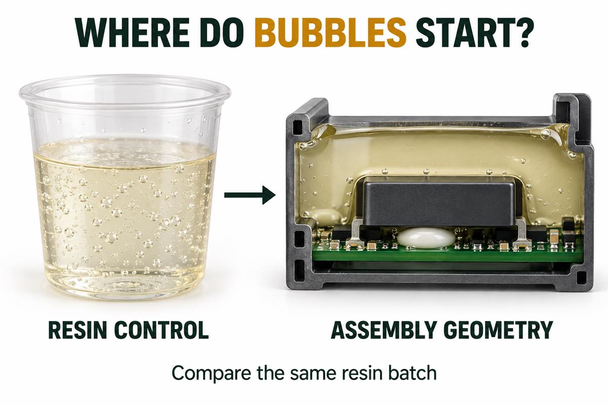
PCB potting bubbles should be traced to the stage where they first appear: mixing, filling, or curing. A bubble-filled mixing cup suggests a different experiment from a clean cup that leaves a pocket beneath a connector. Start with a controlled sample and a record of the process before increasing vacuum or oven temperature.
The practical goal is not merely a smooth top surface. It is a qualified encapsulation process that preserves the assembly’s electrical function and meets its defined insulation, thermal, environmental and visual requirements.
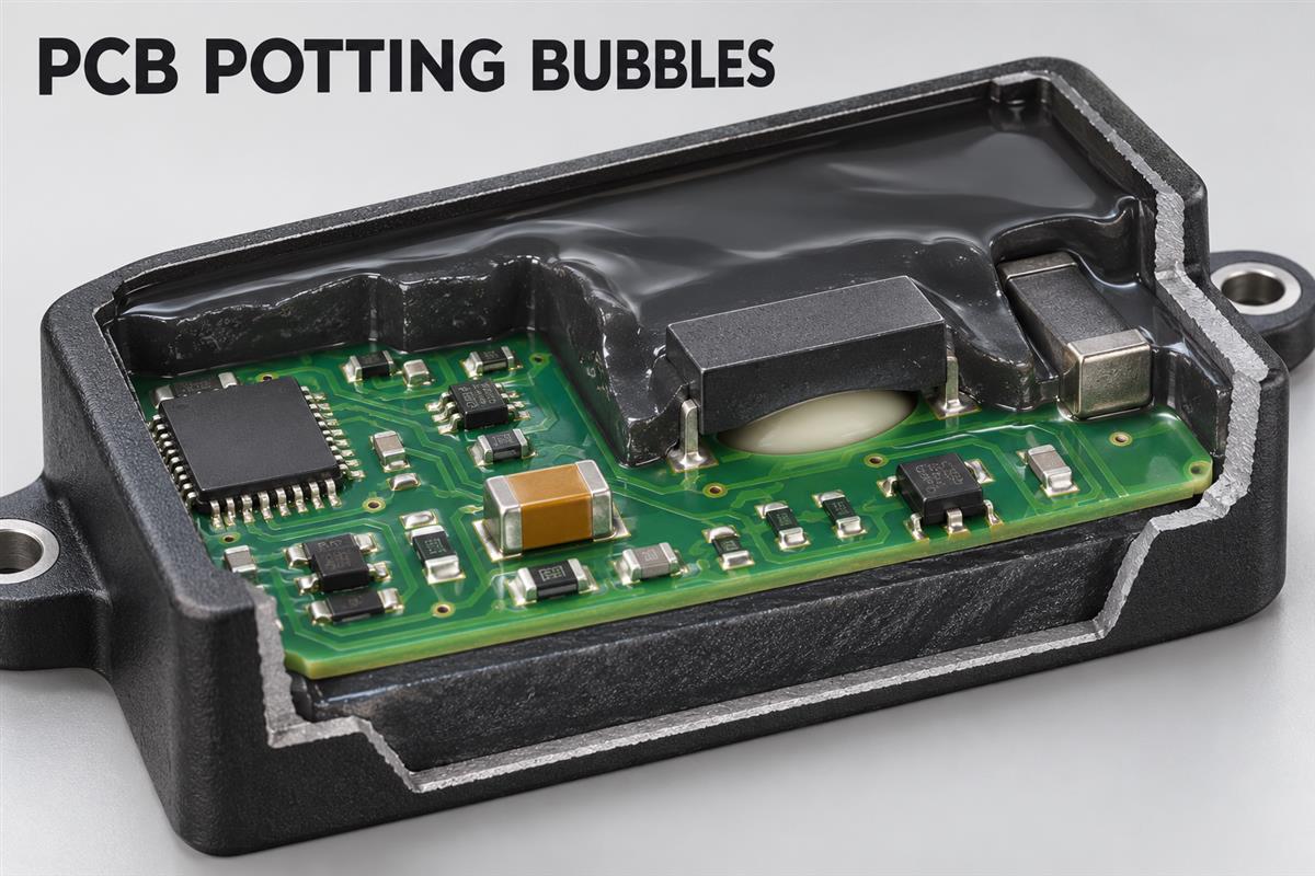
What causes bubbles in PCB potting?
Bubbles may be introduced with the resin, trapped by the assembly’s geometry, or appear during the cure process. Their location and timing help you choose a test, but neither proves the root cause on its own.
| Observation | Working hypothesis | Useful next check |
|---|---|---|
| Fine bubbles already visible in the mixed resin | Air entered during preparation or dispensing | Inspect a retained cup sample before it touches the PCB; compare a controlled mixing or dispensing change |
| Resin looks clear, but pockets repeat beneath the same part | The fill front closes an air escape route | Review a cross-section of the actual assembly and compare an approved fixture orientation |
| Bubbles become visible only after the assembly is heated | Temperature, substrate condition or cure timing is involved | Compare time-stamped samples and measured part temperatures; investigate cleanliness and drying records |
| The last units in a batch show more defects | Material age or dispensing conditions changed | Compare elapsed time from mixing, material temperature, nozzle changes and shot sequence |
| Only one resin lot or enclosure lot is affected | A material or handling difference needs investigation | Hold the lots separately and check storage, preparation and traceability before substitution |
A visible void and an electrical failure can occur together without one having caused the other. Keep failed units and their process records linked. Otherwise, an attractive surface improvement may hide an unresolved electrical defect.
Vacuum degassing vs vacuum potting: which problem does each solve?
Degassing addresses air in the material before filling; vacuum potting addresses the filling operation around the assembly. These are different process locations, so asking a supplier only whether it has a vacuum machine is not enough.
| Question | Resin degassing | Vacuum-assisted potting |
|---|---|---|
| What is being controlled? | The prepared resin before it reaches the product | The environment and fill sequence around the populated assembly |
| Which observation points toward a trial? | Bubbles are present in a retained resin sample | Pockets repeat in difficult-to-fill product geometry |
| What must be recorded? | Material age, container, temperature and approved vacuum cycle | Those variables plus enclosure orientation, fill path and cycle sequence |
| What does it not establish? | That resin will reach every cavity beneath components | That the resin is compatible, correctly proportioned or adequately cured |
Ask the resin and equipment suppliers to confirm a suitable cycle for the actual material and assembly. Record whether pressure is absolute or gauge pressure and record its units. A bare number such as “25 vacuum” is not a transferable process specification. Use rated equipment and its operating procedure; do not improvise a vacuum or pressure vessel.
How do you isolate the source of potting bubbles?
Use a paired control: retain a resin sample and fill a representative assembly from the same preparation. This is a proposed troubleshooting method, not a claim that a particular factory trial has already succeeded.
- Preserve the baseline. Record resin identity, lot, ratio basis, preparation time, ambient conditions and the existing approved fill and cure procedure. Photograph the defect location with a scale.
- Separate material from geometry. Observe the retained resin sample at defined times. If it shows the same defect, investigate preparation and cure first. A clean sample does not clear the material of every possible interaction, but it makes the product geometry worth examining next.
- Map the cavity. Mark the fill point, under-component gaps, air escape routes and prohibited fill areas on a drawing. Identify where two advancing resin fronts could isolate an air pocket.
- Change one approved variable. For example, compare fixture orientation while keeping resin preparation, batch size and cure unchanged. Do not simultaneously change resin, vacuum and temperature and then attribute the result to one of them.
- Verify beyond appearance. Repeat the relevant electrical checks after cure and examine the critical region by the agreed method. Repeat a promising trial sufficiently to assess variation before changing the production instruction.
For example, if a pocket moves when the fixture orientation changes, that observation supports a fill-path hypothesis. It does not prove that all other units are void-free. Document both the improved region and any new pocket created elsewhere.
How should a PCB be prepared before potting?
The assembly needs a compatible cleaning and drying process, defined keepouts, and a fill arrangement that gives displaced air somewhere to go. Preparation is not a generic instruction to bake every board.
The MG Chemicals application guide identifies substrate contamination and moisture as defect risks and calls for compatibility evaluation. It also distinguishes homogeneous preparation from stirring that unnecessarily introduces air. Use the current material instructions together with the limitations of the populated assembly.
- Confirm that the selected cleaner will not damage markings, plastics, sensors or other parts. See the PCB cleaning process for the wider cleaning decision.
- Specify how dryness is established and how long the cleaned assembly may wait before potting. Surface appearance alone is not a documented drying method.
- Mark connector mating areas, switches, pressure ports, optical paths, adjustment points and fasteners that must stay clear.
- Review possible air escape routes with the product owner. Do not drill new vents or enlarge holes without approval: a process convenience may change the enclosure’s sealing function.
Potting is also not the only protection option. If repairability or exposed sensors make encapsulation unsuitable, revisit the broader PCB waterproofing choices before optimizing the wrong process.
Which MG Chemicals 832HD parameters affect a potting trial?
MG Chemicals 832HD is a named example, not a material recommendation for every assembly. Its technical data sheet, version 4.3 dated June 1, 2026, supplies the following values.
| Parameter | Published value | Condition or limitation |
|---|---|---|
| Mix ratio | 1:1 by volume; 1.22:1 by weight | Do not exchange the two measurement bases |
| Mixed viscosity | 4,100 cP | At 25 degrees C |
| Working time | 45 minutes | 100 g sample; varies with volume and geometry |
| Thermal conductivity | 0.3 W/(m K) | At 25 degrees C; ASTM E1461 |
| Hardness | 80 Shore D | ASTM D2240 |
| Glass transition temperature | 41 degrees C | ASTM E1545; not a maximum service-temperature rating |
These are published product data, not universal acceptance limits or guaranteed tolerances. Check the current TDS and SDS, component compatibility, sample geometry and approved cure procedure before use. A different resin needs its own parameter sheet.
Why can heating or curing make a potted PCB fail?
A cure change must be evaluated against both the resin and the complete assembly. The oven setting alone does not describe the temperature history experienced by components or the resin inside a filled enclosure.
A Reddit electronics discussion about 70-degree oven curing describes assemblies that passed before potting and sometimes failed afterward. That is a useful problem statement, not proof that a particular temperature or bubble mechanism caused the failures.
First classify the failure: loss of power, communication failure, sensor offset, intermittent connection or a defined insulation-test failure. Preserve the before-and-after measurements. Then compare an approved unpotted thermal control with potted samples where practical. This can help distinguish exposure to the cure environment from effects associated with encapsulation, although it does not isolate every interaction.
Record actual temperatures at relevant locations in representative trials, not just the oven display. Have the responsible engineer and material supplier review resin mass, assembly temperature limits and the cure profile. The application guide notes that preheating can improve flow while shortening working time; more heat is therefore not a free fix for difficult filling.
How do you inspect and accept a potted PCB?
Acceptance needs a defined region, an inspection method and a decision limit. “No bubbles” without explaining what can be observed is not a usable drawing requirement.
Surface inspection can check visible defects and fill boundaries. It cannot establish the condition of every hidden interface. If an internal region is critical, agree with a qualified inspection provider on a suitable method and demonstrate that it can resolve the defect of concern in that material and geometry. A destructive section samples only its exposed plane; it is not proof about the entire volume.
- Define critical zones: identify where coverage serves insulation, sealing, heat transfer or mechanical support.
- Define observable limits: specify the method, viewing conditions and relevant dimension or coverage criterion, with an approved reference where useful.
- Define electrical evidence: state the required functional and other qualified electrical tests, their limits and when they occur.
- Define disposition: state who may approve a deviation, whether rework is allowed, and how failed units remain traceable.
Do not borrow an arbitrary allowable void percentage from a different product. The acceptance decision belongs to the product’s requirements and validation plan.
What should a potting trial record include?
Keep the following record with the first-article evidence. It gives engineering, production and purchasing a common basis for repeating a result or investigating a return.
- Identity: assembly revision, enclosure revision, unit IDs, resin product, lot, expiry and TDS revision.
- Preparation: cleaning and drying procedure, hold time, masking drawing and inspection result.
- Material: actual component quantities, ratio basis, batch size, initial temperature, mix start and dispensing finish.
- Filling: fixture orientation, nozzle and fill path, fill quantity, approved vacuum cycle if used, pressure units and reference.
- Cure: approved schedule, measured trial temperature history and time before final testing.
- Result: defect map, inspection method, before-and-after electrical results, deviations and approval owner.
When requesting a process change, attach the baseline and changed record together. Highlight one variable and the evidence that supports keeping or rejecting the change.
PCB potting bubbles FAQ
Can ordinary household silicone replace an electronics potting compound?
Do not qualify it by the word “silicone” alone. Check the exact product’s cure chemistry, electrical suitability, adhesion and environmental requirements. A sensor-repair discussion illustrates the substitution question, but community approval does not validate a material for your product.
Can I weigh equal amounts when the resin says 1:1?
Only when the stated ratio is by weight. A volume ratio does not automatically equal a mass ratio. Check the named product’s instructions and set the dispensing or weighing procedure to that basis.
Is 70 degrees C a standard cure temperature for every potted PCB?
No. Use the resin’s approved schedule and check the complete assembly’s limits. A component’s operating-temperature rating is not, by itself, approval of the encapsulation process.
Should I use a torch or heat gun to remove surface bubbles?
Do not improvise concentrated heating on an electronic assembly. It does not establish the condition beneath components and may introduce a new thermal risk. Use the material supplier’s approved de-airing and cure procedure.
Can bubbles be repaired after the compound has cured?
Only under an approved repair method that restores the required function. Covering a surface cavity does not prove that a hidden void has been filled. Preserve a failed sample for investigation before attempting removal.
Does a smooth cured surface prove the inside is void-free?
No. It proves only what the surface inspection can observe. Select and qualify an additional inspection method when the product requires evidence about hidden regions.
Does potting automatically make a product waterproof?
No. The complete enclosure, connector interfaces, keepouts and materials must meet the intended environmental test. Do not assign an ingress rating from the presence of resin alone.
Can final testing replace testing before potting?
It removes a valuable diagnostic checkpoint. A sealed-controller troubleshooting discussion shows the difficulty of reaching a circuit after encapsulation. Agree on pre-potting checks and post-cure tests so a new failure can be localized more effectively.
Need an assembly review before potting?
For a PCB assembly enquiry, send the Gerber files, BOM, placement file, enclosure drawing, proposed resin TDS, quantity and required tests. If you are investigating bubbles, include defect photographs, unit IDs and the trial record above.
Contact PCBtry to discuss the assembly scope and confirm whether the requested encapsulation process and inspection requirements can be supported before placing an order. Keep material selection, acceptance criteria and any special process capability explicit in the quotation.



0 Comments