




PCB backdrilling removes the unused copper barrel of a plated through-hole while leaving the required layer connection intact. It can help a high-speed channel when a via stub is causing unacceptable signal degradation. The useful question is not simply whether a board is fast: it is whether the unused barrel matters to that channel, and whether the fabricator can remove it without damaging the working connection.
Start with the signal’s entry and exit layers, an approved stackup and the channel requirements. Then agree the residual-stub limit, the layers that must remain untouched and the evidence needed to accept the boards. A drawing that says only “backdrill high-speed vias” leaves too much unresolved.

What PCB backdrilling removes, and when it is worth considering
A via stub is the part of a conductive barrel beyond the layers actually used by the connection. Imagine a through-hole on a ten-layer board carrying a signal from L1 to L3. The barrel continuing toward L10 is not part of the intended onward route. It is nevertheless electrically attached, so it can affect the signal.
Backdrilling approaches from the unused end and removes that unwanted barrel with a larger tool. It does not remove the whole via. Altium’s controlled-depth drilling documentation explains this distinction and the relationship between layer pairs and remaining stubs.
For the ordinary drilling and plating sequence, see the PCB via manufacturing guide. Backdrilling is an additional, selective operation, not a replacement for producing a reliable plated connection.
| Design situation | Useful next action | What not to assume |
|---|---|---|
| The channel model or device guidance identifies a problematic unused via barrel | Compare the present transition with a shorter-stub version, including fabrication variation | That removing the stub also fixes reference-plane discontinuities or a poor connector launch |
| A different routing layer or via construction could avoid the long stub | Compare both construction options with the fabricator before freezing layout | That a more complex via structure is automatically cheaper or more reliable |
| No channel requirement or analysis yet explains the need | Ask the signal-integrity owner to establish the requirement first | That every multilayer PCB needs backdrilling |
A data-rate label alone is not a sufficient acceptance rule. Edge behavior, interconnect geometry and the available channel margin matter. Keep the electrical decision with the design owner and the process capability decision with the fabricator; neither should silently substitute for the other.
How the backdrilling workflow protects the working connection
The workflow must carry the same layer identity from design data through CAM preparation, machining and inspection. One wrong side or layer interpretation can destroy the connection the operation was intended to improve.
- Identify the intended connections. List the affected vias or nets and their used layers. Check for branches and connector requirements. A barrel segment that looks unused in one view may still serve another connection.
- Freeze a fabrication stackup. Use the agreed finished construction, not just nominal CAD layer spacing. The fabricator needs to explain how material and lamination variation affect the operation.
- Define each backdrill group. State the entry side, protected layer and residual-stub requirement. Review top-side and bottom-side operations separately; do not infer symmetry from an apparently symmetric board outline.
- Review the removal envelope. A tool larger than the original hole needs room around it. Check nearby conductors, pads and planes using the actual backdrill geometry and the agreed registration allowance.
- Approve the manufacturing interpretation. Have CAM return the operation groups and any exceptions before production. Resolve conflicting drawing notes and drill data rather than allowing the shop to choose between them.
- Machine and verify against the agreed criteria. Confirm that the intended connection remains, unwanted copper has been removed as specified, and inspection records correspond to the correct lot and layer group.
Sierra Circuits’ fabrication guidance discusses backdrill clearances and alternatives such as changing the via construction. Treat a supplier’s published dimensions as that supplier’s guidance, not an interchangeable capability promise from every factory.
How to separate residual stub limits from drill-depth settings
Residual stub is the copper left after drilling; drill depth is a process setting used to remove copper. They are related, but are not the same specification. A fixed travel distance cannot describe the electrical result reliably unless the layer positions, datum and tool geometry are also understood.
Here is a simplified tolerance exercise, not a production recipe. Let D be the distance from the entry surface to the protected connection boundary. Let d be the effective full-diameter copper-removal depth. In this simplified geometry, remaining length r = D – d. The pointed tip of a real drill requires an additional protection check; this equation alone cannot set the machine travel.
Suppose the agreed example range for D is 1.90 to 2.00 mm. The example requires r to remain between 0.10 and 0.30 mm. To protect the nearest possible connection, d must be no more than 1.90 – 0.10 = 1.80 mm. To shorten the farthest possible stub enough, d must be at least 2.00 – 0.30 = 1.70 mm.
The resulting window is 1.70 to 1.80 mm. A nominal 1.75 mm with an assumed effective-depth variation of plus or minus 0.04 mm fits that simplified window. A variation of plus or minus 0.08 mm does not. These numbers are invented for arithmetic only; they are not PCBtry tolerances or a recommended residual-stub range.
The practical lesson is to ask whether the supplier’s demonstrated variation fits the requirement, not just whether a nominal depth can be typed into a machine. If the window is infeasible, revisit the construction, routing or validated electrical limit. Do not relax the requirement without design approval.
There is a second common ambiguity: radius versus diameter. In the cited Altium rule, drill diameter is hole size plus twice the radial oversize. An illustrative 0.30 mm hole plus 0.10 mm radial oversize gives 0.50 mm, not 0.40 mm. Confirm what the exported data and the fabricator mean by each dimension before using it for clearance checks.
What belongs in a backdrill fabrication package
Send enough information for the fabricator to identify the feature, protect the connection and demonstrate the result. A screenshot is useful for discussion, but should not be the only definition of the operation.
| Package item | Question to resolve | Why it matters |
|---|---|---|
| Revision-controlled stackup and layer names | Do CAD, drawing and CAM use the same layer identity and approved thicknesses? | Prevents a correct-looking operation on the wrong construction |
| Affected feature list or machine-readable operation data | Which exact holes belong to each operation group? | Prevents missed holes or unnecessary drilling |
| Entry side and protected connection layer | Which side is the tool entering, and what must remain intact? | Makes the direction and stopping constraint unambiguous |
| Residual-stub acceptance criterion | What is measured, from where, and which limit applies? | Separates the required result from the shop’s machine setup |
| Backdrill diameter interpretation and clearance review | Does the proposed removal envelope clear adjacent copper? | Prevents treating the original small hole as the only affected area |
| Inspection and exception agreement | Which samples, methods and approval records will be supplied? | Stops disagreements appearing only after delivery |
Use one revision identifier across the release package. If the shop changes the stackup or proposes a tool-size adjustment, request a reviewed change record. For the earlier layout checks around plated holes, the annular-ring calculation guide provides context; ordinary annular-ring acceptance does not by itself approve a backdrilled feature.
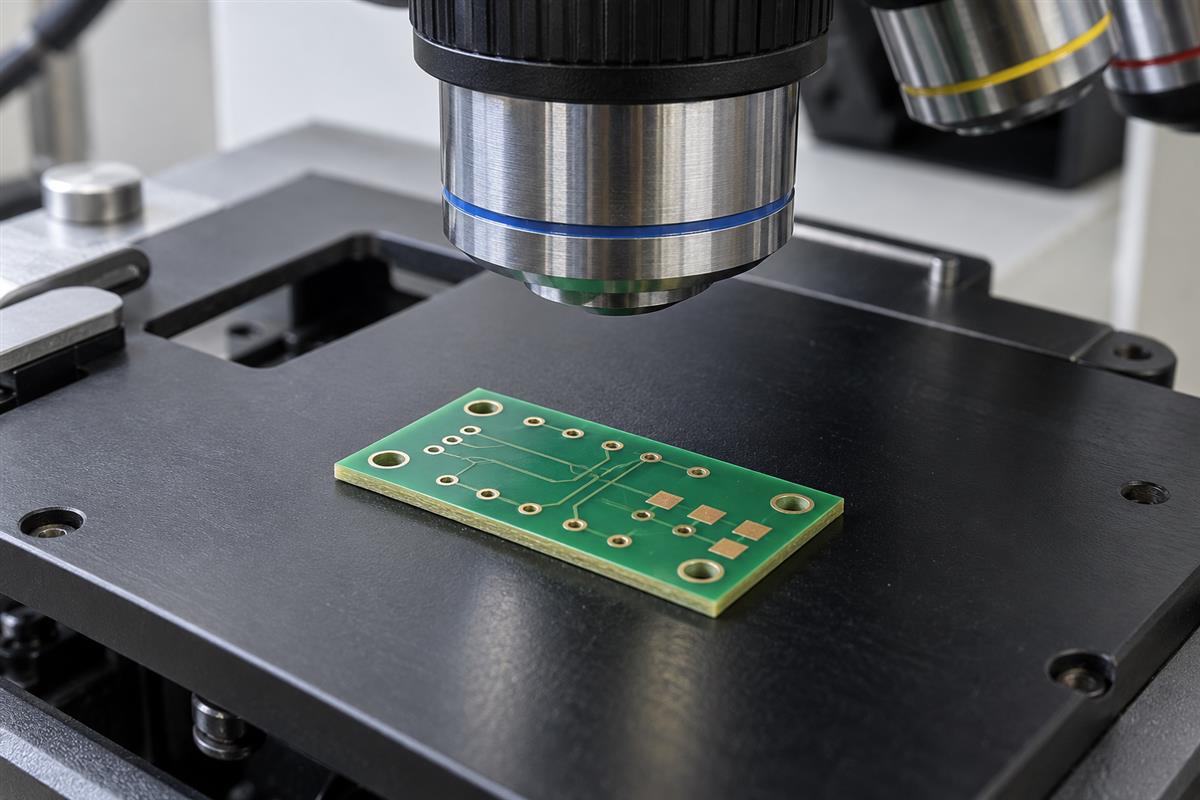
How to check the first lot and compare supplier responses
Accept the lot using agreed evidence, not a clean surface photograph or a general statement that electrical testing passed. The method must answer the particular question being asked.
| Evidence | What it can support | What it does not prove by itself |
|---|---|---|
| Bare-board continuity and isolation result | Whether tested nets meet that electrical test’s connection criteria | That the remaining stub meets a high-speed channel requirement |
| Documented physical section of a representative feature | Local geometry, remaining barrel and condition at the examined location | That every hole across every panel has the same geometry |
| Qualified imaging or targeted electrical characterization | The specific geometry or channel behavior the method has been shown to resolve | Universal coverage without a stated method, resolution and sampling plan |
| Traceable first-lot report | Connection between the approved requirement, measured samples and delivered revision | Long-term capability after unreviewed material or process changes |
In his firsthand discussion of backdrill validation, NPI engineer Joe Clark emphasizes that passing bare-board electrical testing does not establish the required stub geometry. That is why the inspection agreement should be made before ordering.
For a practical quote comparison, ask each supplier to return four items: the operation groups they accepted, any exceptions, the measurement plan and the price/lead-time effect of the specified controls. Compare like-for-like requirements. A lower quote that excludes the required inspection is not yet the same offer.
Release checklist: correct board revision; accepted stackup; identified backdrill groups; agreed limits and measurement definitions; no unresolved CAM exceptions; first-lot evidence linked to the shipment. A mismatch should go back to engineering for disposition, rather than being accepted because the boards power up.
For a project-specific discussion, send the stackup, fabrication data, affected layer pairs, residual-stub requirements and desired inspection scope through PCBtry’s contact page. Ask for capability confirmation and any proposed exceptions before treating the quotation as approval of a particular tolerance.
PCB backdrilling questions
Is a backdrilled via the same as a blind via?
No. Backdrilling starts with an existing plated hole and removes an unused portion of its barrel. A blind via is constructed to connect an outer layer to an internal layer without extending through the whole board. They may address related routing problems, but the manufacturing route and remaining physical opening differ.
Does every high-speed board need it?
No. First determine whether the actual channel has a problematic stub. A design may already use suitable layer transitions or another via structure. Adding an operation without identifying the problem adds requirements and cost without establishing a useful result. Follow the relevant device guidance and channel analysis.
Can I specify zero residual stub?
Do not use zero as an informal way of saying “as short as possible.” The process must preserve the working connection despite variation. Define an electrically justified limit and an acceptable protection margin with the fabricator. If the resulting window is not feasible, change the design or construction rather than relying on a nominal setting.
Will an ordinary continuity test detect an excessive stub?
Not reliably. The wanted connection can remain electrically continuous while an unwanted attached barrel is still too long for the channel. Continuity testing and stub verification answer different questions. Keep both in the acceptance plan when both are required; do not replace the agreed geometry evidence with a generic test certificate.
Can both sides of a board be backdrilled?
Yes, suitable constructions can need operations from both sides. Each side needs a clear entry direction, protected layers and reviewed operation data. Do not assume the same depth works in both directions. The fabricator must confirm the approach for the actual stackup and the connections that remain.
Can I backdrill a finished board with a hand drill?
This is not a sensible repair method for a functional multilayer board. Internal copper is hidden, and depth, registration and tool geometry must be controlled. A visibly centered surface hole does not establish clearance to buried conductors. Discuss an approved rework or replacement route instead of drilling by eye.
Does the smallest available residual stub always give the best order?
Not necessarily. The requirement should satisfy the channel while remaining verifiable and manufacturable. Asking for a tighter value than the design needs can narrow the process window and complicate inspection. Compare the required performance and the supplier’s demonstrated capability, not just the smallest number on a capability page.
What should be reviewed after a stackup change?
Recheck layer positions, protected connections, clearance assumptions, operation data and the inspection agreement. Confirm whether the existing electrical analysis still applies. Even if the layer count stays the same, a thickness or material change can invalidate the interpretation used for the previous backdrill setup.



0 Comments