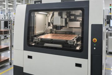
Blog
PCB Laser Drilling Process: Microvias, Cleaning and Inspection
Follow the PCB laser drilling process from stackup review to microvia inspection, with target-pad, cleaning and plating checks for an HDI build.



Follow the PCB laser drilling process from stackup review to microvia inspection, with target-pad, cleaning and plating checks for an HDI build.
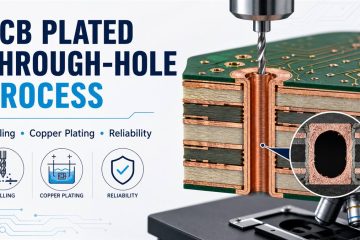
See how plated through holes are drilled, desmeared, activated and copper plated, plus the controls, defects and tests that determine PTH reliability.
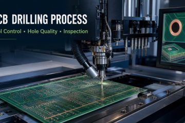
See how PCB drilling uses mechanical and laser processes, with controls for registration, tool wear, smear, hole quality, plating and inspection.
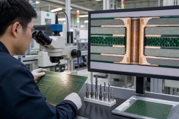
Learn how PCB vias are designed, drilled, desmeared and copper plated, how via treatments differ, and which DFM files and inspection checks prove quality.
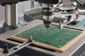
Learn how to choose PCB drill bits, set up the board, drill clean holes, inspect defects and prepare drill data for reliable PCB fabrication.
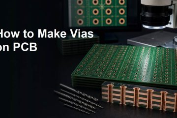
Learn how to make vias on PCB with drilling, copper plating, via types, annular ring checks, aspect ratio limits, and DFM notes before fabrication.
If you have any enquiry about quotation or cooperation, please feel free to email us at sales@pcbtry.com or use the following enquiry form. Oursales representative will contact you within 24 hours. Thank you for your interest in our products.