
Introduction
Whether you’re using a smartphone, operating a computer, or starting your microwave, you are relying on a Printed Circuit Board (PCB). PCBs are hidden inside nearly all electronic devices, serving as their indispensable core skeleton. So, what exactly is the purpose of this “green board” covered in lines and components? Why is it so critically important to modern electronics?
What is a Printed Circuit Board (PCB)?
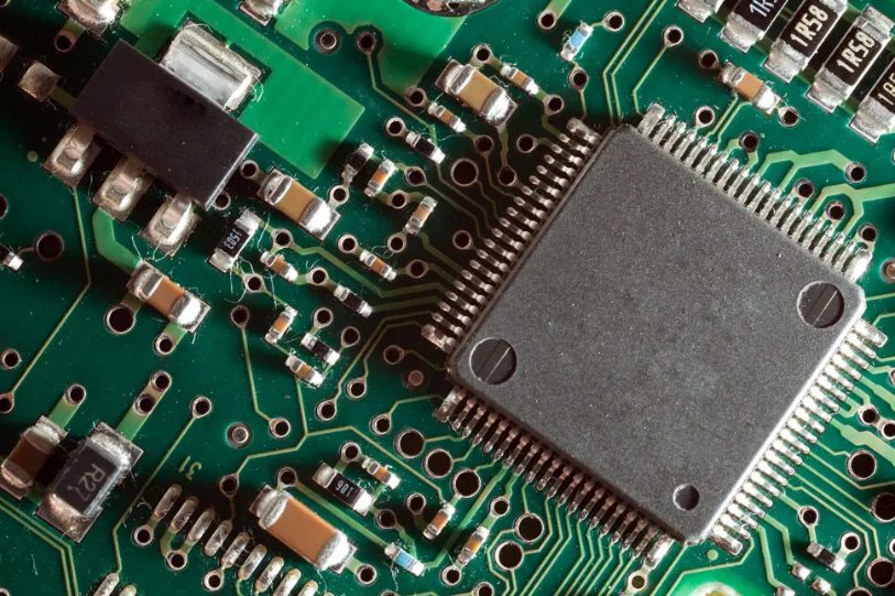
A Printed Circuit Board, or PCB, is a substrate used to mechanically support and electrically connect electronic components. Its core structure consists of precise copper circuit traces printed and etched onto a non-conductive insulating substrate.
You can think of it as the blueprint of a modern city:
- The city’s foundation and blocks are analogous to the PCB’s insulating substrate.
- The individual buildings (homes, shops) are analogous to the various electronic components (chips, resistors, capacitors) soldered onto the PCB.
- The road network connecting all the buildings is analogous to the etched copper traces on the PCB.
All the “functions” of this “city” (computation, communication, display) rely on the orderly and efficient collaboration of components via these circuits.
What is the Purpose of a Printed Circuit Board?
PCBs play multiple critical roles in electronic devices, forming the foundation for their functionality, reliability, and miniaturization.
Provides Mechanical Support
The PCB provides a solid and stable mounting platform for all electronic components. It integrates otherwise loose, independent parts into a compact, organized structure, protecting them from vibration, shock, and physical displacement, thereby significantly enhancing the device’s durability and reliability.
Enables Electrical Connectivity
This is the PCB’s core function. It replaces complex and error-prone wiring with pre-designed conductive pathways (traces), establishing reliable electrical connections between components. This ensures that current and signals travel along precise, designed paths, much like a dedicated “highway system” for electronic signals.
Distributes Signals and Power
The PCB is responsible for distributing power from the source to every component that requires it. Simultaneously, high-speed data signals are transmitted via specifically designed traces (e.g., differential pairs, microstrips). Careful PCB layout is crucial to minimize signal interference, attenuation, and delay, guaranteeing device performance.
Manages Heat Dissipation
Many electronic components generate heat during operation. The PCB, especially those with metal cores or thick copper layers, acts as a heat sink, conducting and dissipating this heat into the surrounding environment. This prevents component damage due to overheating and ensures system stability.
Standardizes and Enables Mass Production
Once a PCB design is finalized, it can be manufactured on a large scale using highly automated processes that are low-cost and ensure high consistency. This revolutionized the manufacturing of electronic devices, making everything from spacecraft to inexpensive toys widely accessible.
Reduces Product Size
Through multi-layer stacking and precise routing techniques, PCBs can implement extremely complex circuit functions within a very small space. This is the direct reason why modern smartphones can be so slim and yet powerful.
PCB Materials
- FR-4: The most commonly used glass-reinforced epoxy laminate, offering good mechanical strength and insulation, suitable for most consumer electronics.
- High-Frequency Laminates: Materials like Rogers, used in 5G communication and radar applications, offer low signal loss.
- Flexible Substrates: Materials like Polyimide, which can bend and flex, are used in wearable devices, camera modules, and other applications with space constraints or moving parts.
PCBs are versatile and play a central role in countless electrical devices, from simple household appliances to complex supercomputers.
Types of Printed Circuit Boards
Understanding different PCB types is essential for electronic product design.
Single-Sided Boards
The conductive copper layer is located only on one side of the insulating substrate. Simple structure and lowest cost, suitable for low-complexity circuits like old radios or calculators.
Double-Sided Boards
Double-sided boards feature copper layers on both sides of the substrate. Designers use “vias” to electrically connect these layers, which provides more routing area. As one of the most common PCB types today, they serve in various consumer electronics and industrial control equipment.
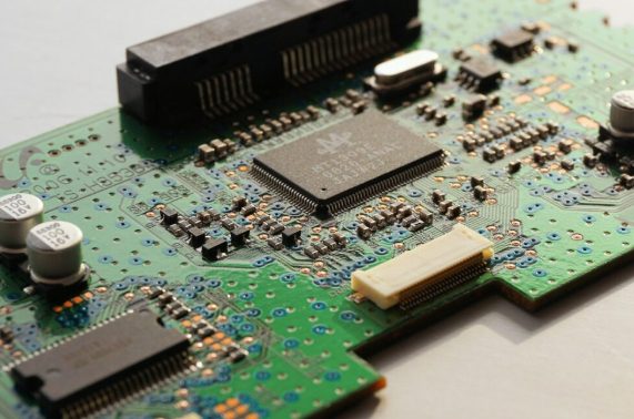
Multi-Layer Boards
Consist of three or more conductive layers laminated together, separated by insulating layers and connected by buried and blind vias. Enable very high density and complex routing; they are the core of modern high-performance computers, smartphones, and communication equipment.
Specialty PCBs
- Flexible PCBs: Made using flexible substrates, they can bend and flex, used in applications requiring dynamic movement or space savings.
- Rigid-Flex PCBs: Combine rigid and flexible boards, offering both support and flexibility, often used in high-end cameras and medical equipment.
- Metal-Clad PCBs: The substrate is metal (e.g., aluminum), offering excellent thermal performance, primarily used in high-power LED lighting and power converters.
How to Select the Right PCB for Your Project
Selecting the appropriate PCB is crucial for project success, cost, and performance.
Number of Layers
Determined by circuit complexity. Simple circuits use single/double-sided boards; complex, high-speed digital, or RF circuits typically require 4, 6, or more layers.
Base Material
Standard applications use cost-effective FR-4. High-frequency/high-speed circuits require specialized high-frequency laminates. High thermal dissipation needs call for metal-clad boards. Flexing requirements necessitate flexible materials.
Size and Shape
The physical dimensions and outline of the PCB must perfectly match the product enclosure. This requires precise planning during the design phase.
Trace Width and Spacing
Determined by current-carrying capacity and signal integrity requirements. High currents require wide traces; high-speed signals require controlled impedance and spacing to prevent crosstalk.
Process Requirements
Factors like surface finish (HASL, ENIG), copper weight, and via types affect the PCB’s solderability, reliability, and final cost.
Summary and Practical Applications
In summary, the Printed Circuit Board is the “urban blueprint” and “neural network” of an electronic product. By providing core functions like mechanical structure, electrical interconnection, and thermal management, it integrates discrete electronic components into a powerful, stable, and miniaturized functional system.
Real-World Examples:
- Smartphone: Inside your phone, the core component is a high-density, multi-layer mainboard PCB, integrating thousands of connections in an area the size of a thumbnail.
- Laptop: Besides the motherboard, the keyboard, touchpad, and display each have their own PCBs.
- Smart TV: The mainboard, power supply board, and logic board are all distinct functional PCBs.
- Automotive: A modern car may contain over a hundred PCBs of various sizes, from the Engine Control Unit (ECU) to parking sensors.
- Wi-Fi Router: The heart of your wireless network is a PCB processing high-speed data.
0 Comments