
Introduction
Light Emitting Diodes, commonly known as LEDs, are an increasingly popular lighting technology across various industries. LEDs are a form of solid-state lighting that uses semiconductors to convert electrical energy into light energy. Compared to traditional bulbs, LEDs can save up to 80% in energy consumption and last up to 25 times longer. Furthermore, LEDs offer other advantages such as compact size and environmental friendliness.
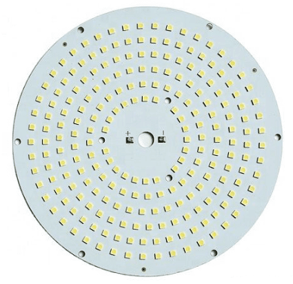
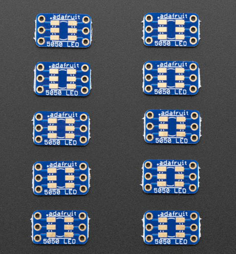
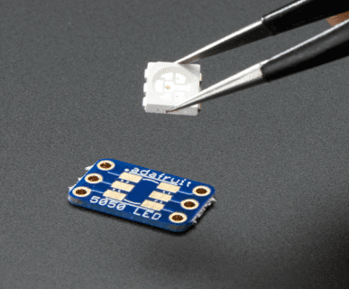
Printed Circuit Board technology plays a crucial role in supporting LEDs. These thin boards, made from materials like fiberglass or metal, are used to electrically connect electronic components. These boards, commonly referred to as PCBs, are essential for many LED applications. They provide physical support for the LEDs and dissipate heat away from the light-emitting chips, thereby enhancing LED performance and preventing damage.
LED Printed Circuit Boards possess many characteristics that enable their ideal performance in applications. In this article, we will introduce some of these characteristics, some applications of LED PCBs, and the benefits of using this technology.
What is an LED PCB?
An LED PCB, short for Light Emitting Diode Printed Circuit Board, is a circuit board specifically designed for mounting and operating LEDs. It is not only the physical substrate for fixing the LEDs but also a critical component that provides electrical connections and heat dissipation for the LEDs.
You can understand it as:
- The “Foundation and Skeleton” of the LED: All LED chips are precisely soldered onto the PCB, forming specific arrays and circuits.
- The “Energy Delivery Network“: The copper traces etched onto the PCB accurately transmit current from the power source to each individual LED.
- The “Heat Manager“: LEDs generate significant heat when illuminated, and the PCB (especially metal-core boards) plays a core role in rapidly conducting this heat away, ensuring the LEDs operate within safe temperature limits, thereby guaranteeing their lifespan and luminous efficacy.
Advantages of LED PCBs
As electronic products become smaller and thinner, the use of LED PCBs is becoming increasingly popular. Using LED PCBs offers various advantages:
- Lightweight with a low-profile form factor
- Dimensional Stability
- Manageable Thermal Expansion
- Excellent Heat Dissipation
- Lower-cost backlighting for membrane switches
- Dust and Moisture Resistance
- Easy integration into complex interface assemblies
- High Efficiency and Low Power Consumption
- Available in various sizes, colors, and intensities
- Can be used in silver-flex and copper-flex membrane switches.
Beyond increasing the light output of luminaires by integrating multiple LED components, there are two main reasons why LED PCBs are so popular:
- Integrating LEDs of different color temperatures or colors onto the same PCB allows for convenient color adjustment and functionality.
- Using boards of different shapes, sizes, and materials enables the creation of various luminaires to meet different lighting requirements.
Why are Metal-Core Substrates Commonly Used for LED PCBs?
Unlike the FR-4 (fiberglass) substrates common in traditional electronics, most high-power LED applications utilize metal-core printed circuit boards, most commonly aluminum substrates.
- Excellent Thermal Conductivity: Aluminum is a good conductor of heat. It quickly absorbs the heat generated by LEDs and dissipates it evenly, preventing chip performance degradation or damage due to overheating.
- High Structural Strength: Metal cores are more robust than FR-4, making them suitable for applications requiring mechanical stability.
- Lightweight: Compared to other metals, aluminum provides good heat dissipation while maintaining a relatively light weight.
A typical aluminum-based LED PCB consists of three layers:
- Circuit Layer: The top layer, made of copper foil, used for etching circuits and soldering LEDs.
- Insulation Layer (Dielectric Layer): The middle layer, made of a special thermally conductive but electrically insulating material, which conducts heat while preventing a short circuit between the circuit and the metal base.
- Base Layer: The bottom layer, which is the aluminum plate, primarily responsible for heat dissipation and structural support.
Aluminum LED Circuit Boards
Aluminum PCBs are the most common type of LED PCB. These boards are mounted on an aluminum alloy base, typically composed of aluminum, magnesium, and silicon. These LED PCB materials are tailored to meet the needs of various applications.
An aluminum PCB consists of multiple layers:
- Base Layer: This layer includes an aluminum alloy plate, serving as the foundation for the rest of the PCB.
- Thermal Insulation Layer: This layer consists of a ceramic polymer that protects the board from thermal and mechanical damage. When current flows through the circuit, this thermal layer absorbs the dissipated heat and transfers it to the aluminum layer for eventual dissipation.
- Circuit Layer: This layer contains the copper circuits laid out according to the LED PCB’s circuit design.
The number of layers on the PCB varies depending on the board’s design.
Aluminum LED PCBs come in various types with different characteristics, making them suitable for a wide range of applications.
- Flexible Aluminum: Flexible LED PCBs are composed of aluminum, polyimide resin, and ceramic fillers, giving them higher flexibility and insulation while retaining aluminum’s thermal conductivity. You can bend these PCBs for connection, eliminating the need for connectors, cables, and other fixtures. They are designed for a one-time bend during installation rather than continuous flexing, unlike standard rigid boards.
- Hybrid Aluminum: These boards are made by fusing an aluminum base with non-thermally conductive materials, such as traditional FR-4 boards. Using these boards can reduce costs and increase rigidity while still providing excellent heat dissipation.
- Multilayer Aluminum: Multilayer aluminum PCBs have more than two layers made of thermally conductive dielectric material. These boards can achieve high performance while still providing effective heat dissipation, although their thermal conduction efficiency is not as high as other types. They differ from simple single and double-layer PCBs.
Benefits of LED Circuit Boards
LED lighting and LED PCBs offer numerous advantages that make them shine in many applications. These benefits include:
- Reduced Power Consumption: According to the U.S. Department of Energy, LEDs use at least 75% less energy than incandescent lighting. Widespread use of LEDs by 2027 could save 348 TWh of electricity, equivalent to about $30 billion in energy cost savings.
- Longer Lifespan: LED lamps have a lifespan of approximately 25,000 hours, which is 25 times longer than incandescent bulbs. Needing fewer replacements saves significant time and cost.
- Higher Efficiency: Incandescent bulbs release about 90% of their energy as heat. LEDs generate very little heat, meaning more energy is used for the desired lighting effect and less is wasted as thermal energy. Non-LED lighting often requires reflectors to direct light, which can trap some light within the fixture. LEDs emit light in a specific direction, making it easier to direct light where needed and ensuring all light exits the fixture.
- Compact Size: LED lamps are much smaller than other types of lights, allowing them to work in tiny devices like smartphones or serve as micro-indicators. They are also versatile enough for large applications like traffic signals and spotlights.
- Mercury-Free: LED lamps do not contain toxic mercury like some other lighting types. This makes them safer, more environmentally friendly, and easier to dispose of.
- No RF Emissions: LED lamps do not emit radio frequencies during operation, meaning they won’t cause interference with other electronic components and devices.
- Environmentally Friendly: LED lamps consume significantly less energy than other bulbs, reducing emissions from power generation. Their longer lifespan also results in less waste.
- Cost Reduction: The increased efficiency and extended life of LEDs lead to cost savings through reduced energy usage and fewer bulb purchases.
Benefits of Aluminum for LED PCBs
Aluminum is one of the most popular materials for LED circuit boards because it possesses many properties well-suited for LED applications. Perhaps the most valuable property of aluminum LED PCBs is their excellent thermal conductivity. Sustained high temperatures can damage electronics and LEDs, shortening their lifespan and degrading performance, including the quality and color of the light. Given these risks, good thermal conductivity – the efficiency with which thermal energy transfers between different locations – is essential for electronic devices. Aluminum has relatively good thermal conductivity, allowing it to draw heat away from components like LEDs.
The thermal conductivity of aluminum allows for mounting more LEDs on a single board. Since LEDs generate heat, mounting too many can lead to excessive heat buildup. However, using an aluminum PCB allows for increasing the LED count without sacrificing performance. Furthermore, the longer electronics operate, the hotter they can become. Improved thermal conductivity enables devices to run for longer periods, even continuously, and extends the overall lifespan of the LEDs and the device.
Other benefits of using aluminum for LED circuit board design are as follows:
- Lower Cost: Aluminum is relatively abundant and easy to refine worldwide, making it cheaper than many other metals. Using aluminum for PCBs is also less expensive than other heat transfer methods like heat sinks. Using aluminum LED PCBs can reduce the overall production cost of the PCB.
- Enhanced Environmental Friendliness: Aluminum is recyclable and non-toxic, reducing the carbon footprint of PCB production. Using aluminum also simplifies and makes the end-of-life disposal of PCBs safer.
- Increased Durability: Aluminum PCBs are more durable than those made of fiberglass or ceramic, making them more resistant to damage during manufacturing and product use. This durability makes them ideal for use in harsh environments.
- Lighter Weight: Aluminum itself is lightweight, making aluminum circuit boards easier to transport and handle. Their light weight and reliable performance make them ideal for vehicles and other similar applications.
Application Areas of LED PCBs
Lighting Sector
This is the most traditional and extensive application area for LED PCBs.
- Residential Lighting:
- LED Bulbs/Tubes: Replacing traditional incandescent and fluorescent lights; the core is an LED module driven by an aluminum PCB, achieving high efficiency and long life.
- Ceiling Lights, Panel Lights: Using large-sized LED PCBs to achieve uniform surface lighting with soft, comfortable light.
- Desk Lamps, Eye-Care Lamps: Precisely control brightness, color temperature, and even achieve flicker-free and blue-light reduction features.
- Smart Lamps: Smart control circuits integrated onto the LED PCB enable complex functions like smartphone app control, voice interaction, dimming, and color changing.
- Commercial & Industrial Lighting:
- Downlights, Spotlights: Commonly used for accent lighting in malls, museums; require high brightness, precise beams, and good heat dissipation, making high-power LED PCBs the ideal choice.
- High Bay Lights, Industrial Luminaires: Provide large-area lighting in factories, warehouses, etc.; demand extremely high heat dissipation and luminous efficacy from the LED PCB.
- Street Lights: Harsh outdoor environments require LED PCBs with excellent waterproofing, dust resistance, lightning protection, and heat dissipation.
- Specialty Lighting:
- Plant Growth Lights: Use LED PCBs to provide specific light wavelengths (e.g., blue, red) needed for plant growth, used in indoor farms, greenhouses, etc.
- Medical Lighting: Used in surgical shadowless lamps, dental lights, skin treatment devices, etc.; require stable, shadow-free light with accurate color temperature, which LED PCBs perfectly fulfill.
- UV Curing Lamps: Use PCBs with UV-LEDs for rapid curing processes in printing, coating, nail art, and other industries.
2. Automotive Industry
Modern cars are becoming “rolling showcases for LEDs.”
- Exterior Lighting:
- Headlights/Matrix Headlights: High-density LED PCBs enable smarter, brighter adaptive high beams that can automatically avoid blinding oncoming drivers.
- Daytime Running Lights (DRLs): Have become part of the car’s signature design; often use flexible LED PCBs to fit complex shapes.
- Full-Width Tail Lights/High-Mount Stop Lights (CHMSL): Use long, linear LED PCBs to create highly distinctive light signals.
- Interior Lighting:
- Ambient Interior Lighting: Install multi-color LED PCBs in dashboards, door panels, footwells, etc., to create a personalized driving experience.
- Instrument Cluster Backlighting: Provide uniform and reliable backlighting for LCD screens and gauges.
3. Consumer Electronics & Appliances
LED PCBs provide the visual interface for human-computer interaction and functional lighting in electronic devices.
- Display Devices:
- TV/Monitor Backlighting: Numerous LED chips arranged on PCBs in direct-lit or edge-lit arrays serve as the light source for LCD screens.
- Laptop/Tablet Backlighting: Ultra-thin LED PCBs are key to achieving slim device profiles.
- Indicator Lights & Panels:
- Power/Status Indicators: The small bright spot found on almost all appliances is backed by a micro LED PCB.
- Appliance Control Panels: Backlighting for displays and buttons on microwaves, washing machines, air conditioners, etc.
4. Advertising & Display
This is the most visual and dazzling application of LED PCBs.
- LED Displays:
- Outdoor Advertising Billboards: Composed of countless modules (each a precise PCB) containing red, green, and blue LEDs assembled together.
- Indoor Fine-Pitch Displays: Used in conference rooms, command centers, broadcasting, etc.; require extremely high precision and heat dissipation from the LED PCB.
- Flexible Curved Screens: Use flexible LED PCBs to create cylindrical, wave-like, and other special-shaped display effects.
- Light Boxes/Signage:
- Store signs, subway signs, illuminated letters, etc., use LED PCBs as the light source for even brightness and long life.
5. Electronics & Telecommunications
In this field, LED PCBs often play more of a “signaling” role rather than “illumination.”
- Signal Indicators: On routers, switches, servers, etc., used to display network status, data transmission, and power conditions.
- Optocouplers: Use LEDs and photosensitive elements on a PCB to achieve isolated transmission of electrical signals, serving as important protective components in power and communication circuits.
6. Cutting-Edge & High-Precision Fields
- Mini/Micro LED: This is the next-generation display technology. It involves the mass transfer of micron-sized LED chips directly onto PCBs (or glass substrates), achieving higher brightness, contrast, and color saturation for high-end TVs, AR/VR devices.
- Wearable Devices: Heart rate monitoring sensors on smart bands/watches; the core is specific wavelength LEDs and receivers integrated onto a tiny flexible PCB.
How is an LED PCB Made?
The manufacturing of an LED PCB is a precise, multi-step process that combines traditional PCB fabrication techniques with special handling for metal-core substrates. Here is the core manufacturing workflow:
1. Design and Planning
Everything starts with circuit design. Engineers use specialized software to draw the circuit schematic, determine LED placement, circuit traces, pad sizes, and drill hole locations. For aluminum substrates, thermal design is paramount, requiring calculations of thermal resistance and heat dissipation paths.
2. Substrate Preparation
Based on the design requirements, an appropriately sized aluminum substrate panel is cut. The aluminum panel is usually pre-laminated with the insulation and copper foil layers.
3. Pattern Transfer
- Copper Surface Cleaning: Ensures the copper foil surface is free of oxidation and contamination.
- Photoresist Application: A uniform layer of ultraviolet-sensitive photoresist is applied to the copper foil.
- Exposure: The designed circuit film is placed over the photoresist-coated board and exposed to UV light. The photoresist under the transparent parts of the film undergoes a chemical reaction, while the parts under the black lines remain unchanged.
- Development: A chemical solution is used to wash away the unexposed (or exposed, depending on positive/negative process) photoresist, thereby creating an etch-resistant protective layer of the circuit pattern on the copper surface.
4. Etching
The board is placed in an etching machine where a chemical solution (e.g., ferric chloride) dissolves the unprotected copper, leaving behind the protected circuit traces. Afterwards, the remaining photoresist is stripped away, revealing the clear copper circuitry.
5. Drilling and Profiling
- Drilling: Holes are drilled at locations requiring component mounting or mechanical fastening. Note: Holes in aluminum substrates are typically mechanically drilled, and due to the insulating layer, these holes are generally not used for inter-layer conduction.
- V-Scoring: If the PCB is designed as a panel, V-shaped grooves are cut between the individual boards to facilitate separation later.
6. Solder Mask and Silkscreen
- Solder Mask: A layer of green insulating ink (solder resist) is applied over the copper traces to prevent short circuits during soldering and oxidation during use. This layer leaves the solder pads exposed.
- Silkscreen: White or other colored ink is printed on top of the solder mask to add characters, logos, and component reference designators, aiding subsequent assembly and repair.
7. Surface Finish
The exposed solder pads (e.g., for LEDs) undergo a surface treatment to enhance solderability and prevent oxidation. Common processes include:
- HASL (Hot Air Solder Leveling): Low cost, widely used.
- ENIG (Electroless Nickel Immersion Gold): High surface flatness, strong oxidation resistance, better for fine-pitch LED pads.
- OSP (Organic Solderability Preservative): Forms an organic protective film on the copper surface; environmentally friendly and low cost.
8. Testing and Inspection
Before leaving the factory, the PCB undergoes rigorous testing, including:
- Electrical Testing: Uses flying probes or a test fixture to check for open or short circuits.
- AOI (Automated Optical Inspection): Uses cameras to inspect for defects in traces, solder mask, and silkscreen.
- Dimensional Inspection: Ensures board dimensions and hole positions meet design requirements.
9. Panel Separation and Packaging
The large panel is separated into individual LED PCBs along the V-score lines. They are then packaged with moisture and shock protection for shipment to the LED assembly factory.
Subsequent Steps: At the LED Assembly Factory
After the PCB is manufactured, it is sent to an LED assembly plant, where SMT (Surface Mount Technology) machines precisely place LED chips and other components onto the pads. The assembly then passes through a reflow oven to solder the components in place, finally becoming a complete LED module or luminaire.
How to Make an LED PCB Board – A DIY Guide
Step-by-Step Instructions
Making your own LED PCB can be an exciting and rewarding project. Here is a step-by-step guide to get you started:
Step 1: Design the LED PCB:
Use PCB design software to create a schematic for your LED circuit and design the PCB layout, considering component placement and signal flow.
Step 2: Select Materials:
Choose a suitable substrate material and copper-clad board based on your project needs.
Step 3: Transfer the Design:
Print your PCB layout onto special transfer paper, then transfer it to the copper-clad board using a heat press or a common household iron.
Step 4: Etch the Board:
Immerse the board in an etching solution (e.g., ferric chloride) to remove the unwanted copper, leaving behind the copper traces.
Step 5: Drill Holes:
Drill holes in the board to accommodate LED chips and other components.
Step 6: Solder Components:
Carefully solder the LED chips and other components onto the board, ensuring solid connections.
Step 7: Test the LED PCB:
Connect the LED PCB to a power source and test the LEDs to ensure they light up correctly.
Conclusion
The LED PCB is the unsung hero of modern lighting technology. It silently carries the light source, manages the energy flow, and, most critically, guards the “lifeline” of the LED – temperature. From intricate circuit design to complex chemical etching and mechanical processing, every high-quality LED PCB embodies advanced materials science and manufacturing craftsmanship. It is these precise structures hidden behind the glow that support the increasingly brilliant and colorful LED world we see today.


0 Comments