
A Ceramic PCB, as the name suggests, is a printed circuit board that uses ceramic material as the substrate. Unlike traditional PCBs that use organic resins (like FR-4) as the base material, ceramic PCBs are sintered from inorganic ceramic materials such as Alumina (Al₂O₃), Aluminum Nitride (AlN), and Beryllium Oxide (BeO) through special processes.
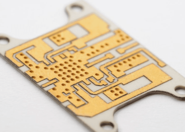
This fundamental difference in material leads to a vast disparity in performance. We can compare a traditional FR-4 PCB to an ordinary asphalt road, while a ceramic PCB is like a high-strength, ultra-flat professional racetrack built for Formula 1 cars. The latter’s stability and performance under high speed, high temperature, and high load are incomparable to the former.
Basic Components of Ceramic PCBs
Let’s examine its basic components.
First is the highly integrated circuit board, which has become an inevitable trend in the advancement of electronic technology. Modern technology and electronics integrate hundreds, thousands, or even millions of transistors and resistors onto a small silicon chip or integrated circuit (commonly known as an IC), forming complex components.
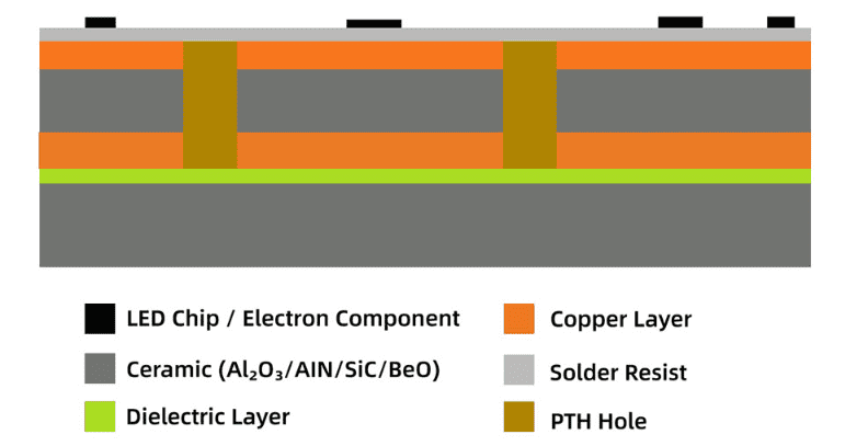
These integrated circuits require a base for building tiny electronic materials and connections, commonly called a substrate. They also need a structure that isolates the circuit from the external environment and turns it into a compact and robust unit, called a package.
Integrated circuits require substrates and packages to maintain their reliability. ICs need insulating materials, and these two components serve exactly that purpose. These packages are then mounted onto printed circuit boards.
Ceramics are known for their insulating properties. The protective characteristics of these advanced ceramic materials are a key reason they are used as substrates and packages. This is also why Ceramic Printed Circuit Boards stand out among their peers.
Due to their excellent thermal conductivity and hermeticity, ceramic PCBs are widely used in power electronics, hybrid microelectronics, electronic packaging, and multi-chip modules. Their excellent electrical conductivity is crucial in applications like power generation that require large currents to pass through the material.
The aerospace and automotive industries are particularly suited for using these PCBs due to their high-power density circuit designs meant for harsh environments.
Ceramic PCB substrate materials are suitable for high-temperature, high-pressure, corrosive, or high-vibration circuit environments. They are applicable in high-temperature scenarios where ordinary PCBs would fail due to their inability to withstand the heat.
What Materials are Used in Ceramic PCBs?
Various materials are used in the production of ceramic PCBs. The two fundamental properties to consider when selecting a ceramic material are its thermal conductivity and Coefficient of Thermal Expansion (CTE).
Alumina (Al₂O₃), Aluminum Nitride (AlN), Beryllium Oxide (BeO), Silicon Carbide (SiC), and Boron Nitride (BN) are some of the ceramic substrate materials used in ceramic PCBs. These ceramic materials share similar physical and chemical characteristics. The three most widely used materials in ceramic PCBs are as follows.
Beryllium Oxide (BeO)
Beryllium Oxide (BeO), historically also known as glucina or glucinium oxide, is derived from beryl or beryllium minerals. It is a white, solid, crystalline inorganic compound.
Apart from good electrical insulation properties, its thermal conductivity [209 to 330 W/(m·K)] is higher than any other non-metal except diamond, and it even surpasses some metals. Beryllium oxide has rigid bonds between its atoms, much like diamond. It transfers heat in the form of vibrations through these strong bonds, resulting in minimal energy loss.
This high-temperature resistant compound has a melting point as high as 2506.85 °C to 2575°C, a boiling point of 3905°C, and a CTE of 7.4 to 8.9 x 10⁻⁶/K. These excellent properties make BeO a valuable resource with broad applications in electronics. Other industries also benefit from its high melting point, superior thermal conductivity, and good resistivity.
Alumina (Al₂O₃)
Alumina is an inorganic compound, also known as aluminum oxide. It is an advanced material composed of aluminum and oxygen. It is typically white but can vary depending on purity, ranging from pink to nearly brown. This compound is odorless, appears as a crystalline powder, but is insoluble in water.
Among all oxide ceramics, alpha-phase alumina has the highest hardness and strength. With an alumina content above 95%, it is an excellent electrical insulator with a resistivity up to about 1×10¹⁴ Ω·cm. Its purity usually ranges from 94% to 99%. It can be easily produced in desired colors, hardness, dimensions, and shapes. As its composition can be altered, it is considered advantageous for engineering production.
This industrial oxide ceramic offers outstanding thermal stability, corrosion resistance, excellent mechanical strength, dielectric strength, and can even form hermetic seals. Common 96% alumina has a thermal conductivity of 25.0 W/(m·K) and a CTE of 4.5 to 10.9 x 10⁻⁶/K. Besides being affordable and cost-effective, it boasts numerous advantages, making its popularity unsurprising.
It is the most commonly used substance in ceramics due to its wide range of applications in electronics, including substrates and packages. It is the material of choice when applications do not have demanding thermal performance requirements. It is one of the most thoroughly researched and comprehensively characterized advanced ceramic materials available today.
Aluminum Nitride (AlN)
Aluminum Nitride (AlN) is a non-oxide, technical-grade semiconductor ceramic material. The compound has a hexagonal crystal structure and is bluish-white in its pure state. Aluminum nitride is a synthetic ceramic compound, typically white or gray, sometimes with a faint yellow tint.
One of the best ceramic substrate materials available today is Aluminum Nitride (AlN). Its resistivity ranges from 10¹⁰ to 10¹² Ω·m, and its thermal conductivity ranges from 80 to 200 W/(m·K), potentially even reaching 300 W/(m·K). Based on these properties alone, it is undoubtedly one of the most attractive and best choices for a PCB substrate material.
It possesses electrical insulation properties and a relatively low CTE of 4 to 6×10⁻⁶/K (between 20 and 1000°C), which is very close to the CTE of silicon wafers. This compound’s CTE value is significantly higher than that of alumina, but it also comes at a higher cost. It is most suitable for use in high-current and high-temperature environments.
What are the Types of Ceramic PCBs?
Ceramic Printed Circuit Boards come in various types and configurations, each designed to meet specific application and performance requirements. Here are some common types of ceramic PCBs:
- Single-Layer Ceramic PCBs: These are basic ceramic PCBs with only a single conductive layer on a ceramic substrate. They are typically used for simple applications requiring high thermal conductivity but not complex circuitry.
- Multilayer Ceramic PCBs: These PCBs consist of multiple layers of ceramic substrates interconnected by conductive traces and vias. Multilayer ceramic PCBs are suitable for complex circuit designs, high-density interconnects, and applications requiring signal integrity.
- Thick Film Ceramic PCBs: This type uses thick film technology to create conductive and resistive traces on the ceramic substrate. Thick film ceramic PCBs are known for their durability and are ideal for harsh environments like automotive and industrial applications.
- Thin Film Ceramic PCBs: Thin film technology involves depositing thin layers of conductive and insulating materials onto the ceramic substrate. Thin film ceramic PCBs offer precise electrical properties and are often used in high-frequency applications like RF and microwave devices.
- Hybrid Ceramic PCBs: These PCBs combine ceramic materials with other materials, such as organic substrates or metal cores. This hybrid approach allows engineers to balance the benefits of ceramics with the advantages of other materials (e.g., cost-effectiveness or specific thermal properties).
- Alumina (Al₂O₃) Ceramic PCBs: Made from alumina, these PCBs are known for their high thermal conductivity, electrical insulation, and mechanical strength. They are suitable for various applications, including power electronics, LED modules, and high-power RF devices.
- Aluminum Nitride (AlN) Ceramic PCBs: AlN ceramic PCBs offer even higher thermal conductivity than alumina, making them ideal for applications where efficient heat dissipation is critical. They are commonly used in high-power electronics and LEDs.
- Beryllium Oxide (BeO) Ceramic PCBs: BeO ceramic PCBs possess extremely high thermal conductivity and are used in applications requiring superior heat dissipation, such as high-power RF amplifiers.
- Silicon Carbide (SiC) Ceramic PCBs: Known for their excellent thermal and electrical properties, as well as their ability to withstand high temperatures and harsh environments, SiC ceramic PCBs are widely used in high-temperature electronics and power electronics.
- LTCC (Low-Temperature Co-fired Ceramic) PCBs: LTCC technology involves co-firing multilayer ceramic substrates at relatively low temperatures. LTCC ceramic PCBs are used in RF modules, sensors, and other miniature devices.
Outstanding Characteristics of Ceramic PCBs: Why Are They So Favored?
The superiority of ceramic PCBs primarily stems from the excellent physical and chemical properties of the ceramic material itself.
- Extremely High Thermal Conductivity: A Revolution in Heat Dissipation
This is the core advantage of ceramic PCBs. Most electronic device failures are related to overheating. The thermal conductivity of Aluminum Nitride (AlN) ceramic is as high as 170-200 W/(m·K), Alumina (96%) is about 24 W/(m·K), while traditional FR-4 material is only about 0.3 W/(m·K). This means ceramic PCBs act like a “superhighway for heat,” rapidly transferring heat generated by high-power chips (such as LEDs, lasers, power ICs) to heat sinks, significantly reducing the chip junction temperature and enhancing product lifespan and reliability. - Matched Coefficient of Thermal Expansion (CTE) with Chips: A Guarantee of Stability
Semiconductor chips (like silicon, gallium arsenide) themselves have a low CTE. If the CTE of the substrate material (like FR-4) differs too much from the chip, huge thermal stress will occur during temperature cycling due to differing rates of expansion and contraction, leading to solder joint cracking and chip damage. The CTE of ceramic PCBs is very close to that of semiconductor chips, ensuring structural integrity and connection reliability even in extreme temperature environments. - Excellent High-Frequency Performance: Guardian of Signal Integrity
In high-frequency circuits, dielectric constant (Dk) and dissipation factor (Df) are crucial. Ceramic PCBs have a low and stable dielectric constant along with an extremely low dissipation factor. This means high-frequency signals experience minimal energy loss and distortion during transmission, making them very suitable for manufacturing high-frequency components like antennas and RF modules. - Strong Mechanical Strength and Chemical Stability: Fearless in Harsh Environments
Ceramic materials are inherently hard, dense, and possess high mechanical strength. They are also corrosion-resistant, resistant to melting, and radiation-resistant, allowing them to operate stably in harsh chemical environments such as high temperatures, high humidity, and strong acids/bases. This makes ceramic PCBs irreplaceable in fields like aerospace, military, and deep-sea exploration. - High Electrical Insulation: The Cornerstone of Safe Operation
Like all ceramic materials, ceramic PCBs are excellent insulators with high breakdown voltage, ensuring safety in high-voltage applications.
A Look into the Manufacturing Processes of Ceramic PCBs
The manufacturing processes for ceramic PCBs are fundamentally different from the “subtractive” method of etching copper foil used in traditional PCBs. They primarily employ the following advanced technologies:
- Thick Film Technology (TFT):
A special metal paste (like gold, silver, palladium-silver) is screen-printed onto the surface of a pre-sintered ceramic substrate. This is then followed by high-temperature firing (usually over 800°C), firmly bonding the metal layer to the ceramic substrate. This process is mature and relatively low-cost. - Thin Film Technology (DPC):
This is a more precise process. First, a metal seed layer (like Titanium/Copper) is deposited onto the ceramic substrate via magnetron sputtering. Then, a circuit pattern is formed through photolithography and development. The copper layer is then thickened by electroplating. Finally, etching removes the excess seed layer. Thin film technology can achieve finer line widths and spacing (down to below 10μm) and is the preferred choice for high-end devices like lasers and microwave circuits. - Direct Bonded Copper (DBC) / Active Metal Brazing (AMB) Technology:
This process involves directly bonding a copper foil to the surface of alumina or aluminum nitride ceramic through a high-temperature eutectic reaction (typically around 1065°C). It offers high bond strength and a thick copper layer (usually 100-300μm), capable of carrying high currents. Its derivative technology, Active Metal Brazing (AMB), provides even higher bond strength and is the standard technology for manufacturing high-power IGBT modules.
Wide Application Fields of Ceramic PCBs
Leveraging their exceptional properties, ceramic PCBs have become the “heart” components in numerous high-tech fields:
- High-Power LED Lighting: Especially for automotive headlights, UV LEDs, and plant growth lights, ceramic PCBs are key to solving their heat dissipation bottlenecks.
- Power Semiconductor Modules: Core IGBT modules in new energy vehicle motor controllers and rail transit converters use DBC/AMB ceramic PCBs as insulating and heat-dissipating substrates.
- RF and Microwave Communication: 5G/6G base station antennas, power amplifiers, and filters extensively use ceramic PCBs to ensure low-loss transmission of high-frequency signals.
- Aerospace and Defense: Equipment like radar systems, missile guidance, and satellite communication that need to operate in extreme environments rely on the high reliability of ceramic PCBs as the only choice.
- Medical Electronics: Implantable medical devices and medical imaging systems (like CT detectors) demand extremely high stability and biocompatibility, making ceramic PCBs an ideal carrier.
- Sensors and MEMS: High-temperature pressure sensors, gas sensors, etc., utilize the heat resistance and stability of ceramic PCBs.
When is it Ideal to Use Ceramic PCBs?
Ceramic PCBs can be used in a variety of applications, but they are not a universal solution. Considering various factors, they might not be suitable for all situations.
Understanding the factors that determine whether a ceramic PCB is suitable for your project or application is crucial. Some factors to consider when deciding whether to use a ceramic PCB include its cost, weight, and thermal conductivity.
They are corrosion-resistant, have a low CTE, and can be made into very thin layers with high aspect ratios. Consequently, they are lighter and offer better thermal conductivity, making them ideal for applications where size, weight, and heat transfer are critical.
Their high thermal conductivity plays a significant role when multilayer boards are needed. Internal circuit layers and surfaces will avoid hot spots. This makes them highly suitable for applications requiring high temperatures, such as in automotive or aerospace industries. Switching to ceramic PCBs can significantly improve the reliability of mechanical equipment, especially for devices used in the military and heavy industrial equipment sectors.
Generally, ceramic PCBs can be more expensive than traditional PCBs. Despite the cost, they offer a range of advantages that make them an excellent choice for specific applications.
Conclusion
From high-power LEDs illuminating the future, to the “three-electric” systems driving new energy vehicles, to the 5G networks connecting everything, ceramic PCBs, as a fundamental and strategic new material, are silently supporting the rapid development of modern technology behind the scenes with their unparalleled performance advantages. They are not only the solution to heat dissipation and reliability challenges but also a key bridge to a future of higher performance, greater miniaturization, and smarter electronics. As our pursuit of electronic device performance knows no bounds, the importance of ceramic PCBs will undoubtedly continue to grow.
For over 60 years, Beryllium Oxide has demonstrated exceptional chemical and thermal stability under demanding conditions and environments. In PCB applications exposed to high temperatures or where high-density PCBs have space constraints, BeO can be used to provide air or liquid cooling.


0 Comments