




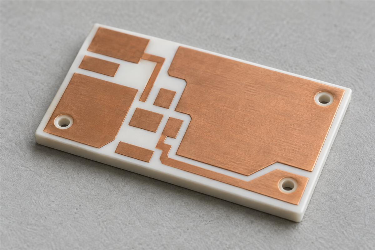
A ceramic PCB is a circuit built on a ceramic insulating base rather than a conventional glass-epoxy laminate. Its metal traces carry electrical current; the ceramic supports those traces, provides electrical separation, and conducts heat through the structure. Alumina, aluminum nitride, and silicon nitride are important substrate options, but the material name alone does not tell you how cool a finished assembly will run.
The useful question is not simply which ceramic has the highest thermal conductivity. It is which part of the heat path is limiting your design. A better substrate may help, or a poor attachment layer, small contact area, or inadequate heat sink may dominate the result. Start with the complete assembly, then choose a material and construction that address its actual constraint.
How Heat Moves Through a Ceramic PCB
Heat travels from the active device through its attachment and substrate toward a cooler surface and eventually the surroundings. Electrical insulation does not mean thermal insulation: a suitable ceramic can resist electrical current while allowing useful heat flow. Copper provides the circuit connections and also spreads heat, but it does not replace the ceramic’s insulating function.
For a simplified power assembly, trace this route: device or package, attachment layer, top metallization, ceramic, backside construction, thermal interface, and heat sink or cold plate. Not every product contains every layer. Some heat also leaves through the package top, leads, or surrounding air. Texas Instruments’ thermal-performance explanation shows why package-to-board and board-to-environment paths must be considered together.
| Part of the path | What to establish | A misleading shortcut |
|---|---|---|
| Heat source | Actual dissipated power, footprint, duty cycle, and allowable device temperature | Using the product’s electrical output power as heat loss |
| Device attachment | Attachment material, coverage, thickness, and acceptable voiding | Assuming every mounted component transfers heat equally |
| Metal and ceramic | Finished construction, heat-spreading area, ceramic grade and thickness | Using bulk conductivity as the whole board’s thermal resistance |
| Board-to-cooler interface | Contact area, flatness, interface material, and approved mounting conditions | Assuming two apparently flat surfaces make perfect contact |
| Heat rejection | Cooler temperature, airflow or coolant conditions, and enclosure constraints | Expecting a ceramic tile to remove heat without a cooler destination |
For example, a converter delivering 100 W does not necessarily dissipate 100 W into its board. Use measured or calculated component losses at the operating point. Likewise, a 20 mm-wide substrate does not mean heat enters uniformly across its entire area: a small die creates a concentrated source, and the resulting spreading problem needs more than a single area value.
Choose the Ceramic for the Constraint, Not the Label
Choose a candidate material by the combination of thermal, electrical, mechanical, and assembly requirements it must satisfy. Then verify the exact grade and metallized construction. A thermal-conductivity advantage is useful only if it improves a limiting part of your assembly.
| Candidate | Reason to evaluate it | Question that decides the next step |
|---|---|---|
| Alumina, Al2O3 | A practical starting candidate for ceramic insulation and an established circuit construction | Does the proposed grade and thickness meet the calculated temperature budget at an acceptable cost? |
| Aluminum nitride, AlN | A candidate where heat flow through the ceramic is a substantial limitation | How much does the complete assembly improve, rather than just the material’s conductivity number? |
| Silicon nitride, Si3N4 | A candidate for power constructions where thermal and mechanical requirements must be balanced | Is there qualification evidence for the proposed ceramic, copper, joining system, and load cycle? |
As specific supplier examples, Rogers’ DBC page lists 24 W/(m K) for alumina and 180/230 W/(m K) for AlN. Its AMB page describes copper brazed to silicon nitride and gives 90 W/(m K) for that product example. These are not universal specifications for all ceramics or a statement of PCBtry’s available grades. Obtain the proposed material datasheet and its measurement conditions.
Keep material and construction separate
AlN names a ceramic material; DBC and AMB name joining approaches. They answer different questions. A quote must identify both what the insulating base is and how the conductive structure is made. A fine-pattern circuit, thick-copper power substrate, and co-fired multilayer package should not be treated as interchangeable simply because each is called a ceramic PCB.
For the production-route details, use the ceramic PCB manufacturing process guide. For material selection here, request the finished cross-section, not just a label such as “premium ceramic.”
Do not turn one property into a reliability guarantee
Thermal conductivity measures heat conduction within the material. Thermal expansion describes dimensional change with temperature. Neither by itself proves that copper, ceramic, solder, and mounted components will survive the required cycles together. Similarly, RF suitability requires dielectric data at the relevant frequency, while electrical isolation requires the actual geometry, environment, and applicable test conditions. A material comparison is a starting point, not a qualification report.
Estimate the Substrate Temperature Drop
A simple conduction calculation helps you estimate whether the ceramic layer is worth improving. For steady, one-dimensional heat flow through a uniform layer, use R = t / (k A), followed by temperature difference = P R. This is a screening model for that layer, not a prediction of semiconductor junction temperature.
- t: layer thickness in meters.
- k: thermal conductivity in W/(m K).
- A: assumed through-flow area in square meters.
- R: thermal resistance in K/W.
- P: heat passing through that layer in watts.
Consider an illustrative uniform layer 0.50 mm thick with an assumed 10 mm by 10 mm heat-flow area and conductivity of 25 W/(m K). These are hypothetical calculation inputs, not a quoted material specification or measured board result.
- Convert thickness: 0.50 mm = 0.00050 m.
- Convert area: 10 mm by 10 mm = 0.00010 m2.
- Calculate resistance: 0.00050 / (25 x 0.00010) = 0.20 K/W.
- For 10 W through this layer, its temperature drop is 10 x 0.20 = 2 K, equivalent to a 2-degree Celsius temperature difference.
Now substitute a hypothetical conductivity of 150 W/(m K), leaving thickness and area unchanged. The layer resistance becomes approximately 0.033 K/W, and its drop at 10 W is approximately 0.33 K. The improvement is about 1.67 K across this layer under these assumptions.
Why does this distinction matter? Suppose all other elements in the same simplified series path add 1.8 K/W. Total resistance changes from 2.0 to about 1.833 K/W, a reduction of roughly 8.3%, not sixfold. The ceramic conductivity improved sixfold; the complete path did not. This is an example of system reasoning, not a prediction for a real package.
Know when to stop using this shortcut
The model assumes a uniform cross-section, constant material property, and a known heat flow. Small chips on large copper areas introduce spreading; pulsed loads introduce transient behavior; multiple devices interact; interfaces introduce additional resistance. Do not insert the entire board area merely because it gives a favorable answer. Use an appropriate thermal model and measurements when these effects matter, and distinguish device junction temperature from a surface temperature measurement.
Check the Interfaces Before Upgrading the Material
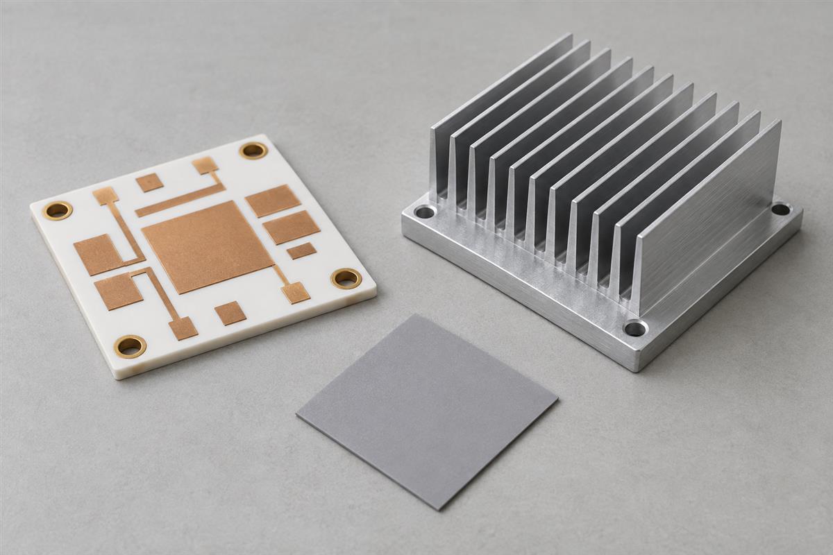
Before paying for a higher-conductivity ceramic, inspect the interfaces connecting the board to its heat source and cooling system. An interface that is too thick, poorly seated, or unsuitable for the gap can consume the temperature budget saved by the new substrate.
Laird’s Thermal Management 101 distinguishes resistance through the interface material from contact resistance at its surfaces. Its practical implication is straightforward: the highest conductivity on a datasheet is not automatically the lowest resistance in the installed joint.
- Identify the actual gap. Include flatness and assembly tolerances, not only nominal CAD dimensions.
- Use installed thickness. Where a material compresses, evaluate its specified behavior under the approved assembly conditions.
- Check support and loading. Do not increase clamp force indiscriminately to improve contact. Obtain an approved mounting method for the brittle substrate and surrounding assembly.
- Check attachment quality. Review the specified bond coverage, process, and inspection evidence where poor attachment could create a hot spot.
- Keep electrical requirements separate. Exposed copper, edges, spacing, and insulation requirements remain important even if the ceramic itself is an insulator.
- Check the cooler. A hot cold plate or insufficient airflow cannot be corrected solely by changing the board material.
In a hypothetical prototype, changing the cooler interface while keeping the ceramic unchanged produces a larger temperature improvement than the proposed substrate upgrade. That result would point toward the interface as a design priority. It would not prove that the alternative ceramic has no value under a different load, geometry, or environment. Change one variable at a time where practical so the comparison answers a specific question.
Turn a Material Choice into a Prototype Review
A useful material decision ends with a testable construction and defined operating conditions. It should not end with “use AlN” or “use ceramic.” The following sequence helps engineering and purchasing compare the same proposal.
- Define the operating case. List each major heat source, expected losses, duty cycle, surrounding temperature, cooling conditions, and temperature limits.
- Draw the heat path. Identify package, attachment, metal, ceramic, interfaces, and cooler. Mark unknown thicknesses or contact conditions for confirmation.
- Screen candidate constructions. Compare material grade, thickness, copper construction, electrical requirements, and mechanical constraints. Use calculations only within their stated assumptions.
- Agree on prototype measurements. Define measurement locations, instruments, stabilization criteria, load points, and ambient or coolant conditions before comparing samples.
- Compare results against limits. Keep the device’s specified temperature limit and required design margin distinct from a convenient board-surface measurement. Include measurement uncertainty in close decisions.
- Release the confirmed specification. Record the selected grade, construction, attachment, mounting method, inspection requirements, and unresolved risks. A material substitution needs review if it changes these assumptions.
For an initial discussion, prepare circuit data, a dimensioned drawing, candidate substrate and thickness, copper requirements, heat-source locations and losses, cooling arrangement, electrical isolation requirements, assembly method, quantities, and the intended qualification conditions. Mark estimates as estimates. Missing thermal inputs are better exposed early than hidden inside a supplier’s assumed construction.
Send this package through PCBtry’s contact page or email sales@pcbtry.com. Ask which construction can be supported and which details need engineering confirmation before a quotation is finalized. This gives the supplier a specific problem to evaluate rather than an open-ended request for the “best ceramic.”
Ceramic PCB Selection Questions
Does the ceramic carry electrical current?
In the insulating substrate constructions discussed here, circuit current flows through the metal features, not through the ceramic base. The ceramic separates conductors while supporting heat transfer. Do not generalize this description to every material called a ceramic; its electrical behavior must be established from the actual grade.
Does a ceramic PCB still need a heat sink?
It depends on heat loss, allowable temperature, and the complete cooling path. Ceramic can improve conduction through the substrate, but heat must still leave the assembly. Some low-loss designs can reject enough heat without a dedicated sink; higher-loss designs need an engineered cooling arrangement.
Is AlN always better than alumina?
No. Its thermal advantage may be valuable when the ceramic layer limits performance. If another interface dominates, the improvement may be smaller than expected. Compare the exact grades and finished constructions, then weigh the measured benefit against cost, availability, and qualification needs.
Are DBC and AMB ceramic materials?
No. They describe ways of joining copper to ceramic. The substrate material and joining route should both be specified. Asking only for DBC or only for AlN leaves important parts of the finished construction undefined.
Can I calculate junction temperature from ceramic conductivity?
Not from conductivity alone. You also need heat losses, dimensions, package behavior, interfaces, cooling conditions, and relevant parallel paths. The simple layer example above estimates only a temperature difference across a hypothetical layer. Use the device manufacturer’s thermal guidance for interpreting its junction temperature.
Is a white circuit substrate definitely alumina?
No. Appearance is not a reliable material identification method. Use the supplier’s grade designation, drawing, and traceability records. A photograph also cannot establish dielectric strength, internal defects, or a thermal-conductivity value.
Should BeO be treated as an ordinary prototype material?
No. Beryllium oxide requires a specialized safety assessment. OSHA identifies health risks from beryllium-containing exposures. Do not drill, grind, or sand an unidentified ceramic or a known BeO part as an informal workshop modification. Consult the material safety documentation and qualified safety personnel.
What makes two ceramic PCB quotes comparable?
They must describe equivalent material grades, dimensions, metallization, finishes, assembly interfaces, inspection scope, and quantities. When thermal performance is part of the requirement, include the same load and cooling assumptions. Comparing prices for different constructions does not identify the better value.



0 Comments