




High-frequency PCB design starts with a measurable RF requirement, not a universal trace width or a rule that every board needs an exotic laminate. Define the operating band, acceptable loss and reflection, reference impedance, and measurement endpoints. Then select the material and transmission-line geometry together, review every transition, and verify the manufactured path against those requirements.
This guide focuses on RF paths: the routes carrying signals between connectors, matching networks, filters, amplifiers and antennas. Digital edge timing is a related but different problem; use the high-speed PCB layout guide for timing and digital return-path checks. A mixed-signal board needs both reviews.
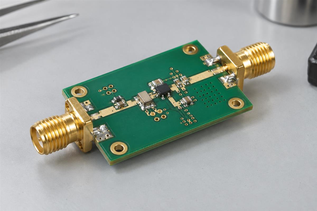
Start With an RF Requirement Sheet
Write down what the RF path must achieve before choosing its stackup. A frequency label alone does not tell you whether a layout will work: line length, bandwidth, loss allowance and phase sensitivity also matter.
Think of the trace as a structure that guides an electromagnetic wave, rather than an ideal wire. Its behavior depends on the conductor and its surrounding dielectric and reference metal. As the route becomes electrically longer, a connector pad, gap in the reference plane or change in geometry can become a significant part of the circuit.
There is no useful universal rule that PCB design suddenly becomes difficult at exactly 1 GHz. A short interconnect and a long precision feed network can have very different requirements at the same frequency. Start with the device requirements and the complete signal path.
| Requirement | What to record | Why it changes the design |
|---|---|---|
| Operating band | Lowest and highest operating frequencies; relevant out-of-band behavior | A center-frequency check can miss a band-edge failure. |
| Reference impedance | System port impedance and any intentional matching sections | Not every pad or matching element is a uniform 50-ohm line. |
| Transmission limit | Maximum insertion loss, or gain requirements for an active path | Sets the allowance for conductors, dielectric, launches and components. |
| Reflection limit | Required input/output return loss across the band | Determines acceptable mismatch, not just nominal trace impedance. |
| Phase and isolation | Phase balance, delay variation or coupling limits where relevant | An amplitude-only test may miss a beamforming or interference problem. |
| Test boundary | Connector faces, probe tips or defined on-board reference planes | Makes the measured result comparable with the simulation. |
| Operating conditions | Power, bias, temperature and enclosure state | A small-signal room-temperature result is not every operating condition. |
For example, “low-loss RF board” is not an acceptance criterion. “Measure the passive path between these two connector reference planes across the specified band, with the unused ports terminated, and compare it with the attached limits” is actionable. The project owner must supply those limits; a fabricator cannot infer them from the board color or material brand.
Choose Materials Against the Actual Loss Budget
Select a laminate using the permitted RF loss, stability and manufacturing requirements. FR-4 is not automatically forbidden, and a premium RF material does not automatically make the whole path acceptable.
A short route with a forgiving loss allowance may be feasible on a suitably characterized FR-4 construction. A longer, higher-frequency or phase-sensitive route may need a lower-loss, more tightly characterized material. Compare the proposed construction at the relevant frequency and length instead of comparing material names alone.
Dk, or relative permittivity, affects the field distribution, electrical length and impedance. Df, or dissipation factor, describes dielectric loss under stated test conditions. Neither is a complete prediction of finished-board insertion loss: copper roughness, trace geometry, conductor loss, transitions and connected components also contribute.
Ask which Dk value belongs in the design model. A datasheet’s process-control Dk and a design Dk can come from different methods and should not be exchanged without understanding their purpose. Rogers also distinguishes material families: its products are not all PTFE, and the lowest Dk is not necessarily the right choice for a compact RF circuit. See Rogers’ explanation of low-loss laminate formulations.
Before approving a substitution, compare the actual grade, dielectric thickness, available copper foil, Dk/Df conditions, dimensional behavior and fabrication compatibility. A purchasing description such as “Rogers or equivalent” leaves too much unresolved when RF response depends on the construction.
Separate Material Loss From the Whole-Path Result
Suppose a prototype misses its insertion-loss limit. Changing the laminate may help if dielectric loss is a significant contributor, but it will not repair a poorly matched connector launch. First compare the model and measurement at the same endpoints, then isolate the route, launches and components. Keep a loss allocation for each section, with a margin appropriate to manufacturing variation.
Adding individual loss values in decibels is a useful first budget when the connected sections are reasonably matched. It is not a substitute for cascading their S-parameter models when reflections interact. Otherwise, a neat spreadsheet can hide frequency-dependent ripple.
Set the Transmission Line Before Routing
Choose the line structure and obtain an achievable stackup before fixing the RF trace width. Copying a width from another board is unreliable when its dielectric height, copper thickness, ground clearance or solder-mask treatment differs.
| Structure | What forms the line | Review before use |
|---|---|---|
| Microstrip | An outer-layer trace over a reference plane | Dielectric height, surface environment, mask and nearby metal |
| Stripline | A trace within dielectric between reference planes | Layer transitions, buried routing access and the actual dielectric construction |
| Grounded coplanar waveguide | A signal trace with adjacent ground and a ground reference below | Signal-to-ground gaps, ground connections, launch geometry and fabrication tolerances |
The Analog Devices RF layout guidance explains these structures and the importance of the ground reference. Treat dimensional examples as examples, not universal design rules.
- Identify the route’s reference. Mark the ground layer and inspect openings, connector cutouts and transitions along the entire route.
- Obtain the proposed construction. Ask for dielectric thicknesses, copper thickness assumptions and the material model used for impedance calculations.
- Solve the geometry. Use an appropriate field solver or a fabricator-reviewed calculation for the actual line structure. Include coplanar gaps and mask where applicable.
- Check production tolerance. Review how the permitted width, gap and dielectric variations affect impedance. Nominal agreement alone does not describe the production range.
- Freeze the approved dimensions. Record which changes require engineering approval, including laminate substitutions and impedance-driven trace adjustments.
Layer count is a result of routing, reference-plane, isolation, power and manufacturing needs. Fewer layers are not an RF objective by themselves. If six layers are under consideration, the six-layer RF stackup review covers that specific decision.
Review Launches, Vias and Coupling as Part of the RF Path
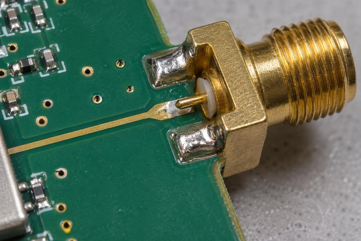
A well-controlled straight trace can still fail at its connector, component pad or layer transition. Review the complete route rather than treating the nominal impedance calculation as proof of RF performance.
At an edge connector, check the manufacturer’s footprint against the actual board thickness and stackup. The center contact, signal pad, nearby ground, solder joint and reference-plane arrangement form one transition. A footprint copied from a different board may be mechanically solderable but electrically unsuitable.
At a signal via, inspect the pad, antipad, unused barrel and nearby reference connections. A shorter unused stub can be useful, but blind vias or backdrilling are not automatically required on every RF design. Compare the transition model across the intended band and ask the fabricator whether the proposed structure is achievable.
Ground stitching is not a substitute for a continuous reference. Keep the local return connection appropriate to the transition, and determine via spacing using the frequency range, geometry and electromagnetic behavior. Avoid adopting a single fence pitch as a rule for all boards.
Coupling also needs a path-level review. Look for long parallel runs, sensitive receiver inputs near strong transmitters, and shared supply or reference paths. More separation may reduce direct coupling, but it does not automatically resolve conducted noise. Use the actual component reference design for biasing and decoupling, then review changes in placement and connection inductance.
For a layout review, mark three places on the drawing: the connector launch, the most complex transition, and the closest aggressor-to-victim region. These deserve more attention than a blanket instruction to “avoid every right-angle bend.” Model electrically significant discontinuities; do not assume a cosmetically smooth route is a validated one.
Read RF Measurements Without Confusing Loss and Reflection
S11 describes input reflection; S21 describes forward transmission with the other port appropriately terminated. They answer different questions, so a good result for one does not establish a good result for the other.
A vector network analyzer measures the amplitude and phase relationships between incident, reflected and transmitted waves. Keysight’s measurement-parameter reference identifies S11 and S22 as port reflections and S21 and S12 as transmission parameters.
A Small Example You Can Check
For a passive two-port path with equal real reference impedances and matched termination at the other port:
- S11 = -20 dB: the reflected-wave magnitude ratio is 10(-20/20) = 0.1. The reflected power fraction is 0.12 = 0.01, or 1%.
- Return loss = 20 dB: this is the positive return-loss expression of that same reflection. It is not 20 dB of forward insertion loss.
- S21 = -1 dB: the transmitted power fraction is 10(-1/10), about 79.4% under these matched-reference conditions. The corresponding insertion loss is 1 dB.
The two readings describe how much comes back and how much gets through. Neither number is a universal pass limit. Also, the power not transmitted is not necessarily all dielectric heating: reflection and other mechanisms can contribute. Keysight explains the return-loss sign convention in its reflection measurement tutorial.
Make the Test Boundary Match the Design Boundary
A measurement at cable ends can include the board’s connectors and launches. A simulation that starts at the trace after the launch does not include the same structure. Comparing them directly can make a good model look wrong or conceal a bad transition.
Define the reference planes in the test drawing. Calibrate using the instrument’s suitable procedure and standards, and account for any fixture between those planes and the intended device. De-embedding uses a characterized fixture model to remove its contribution. Simple port extension is not a general cure for fixture mismatch; Keysight’s fixture-removal guidance explains that distinction.
Save the unprocessed result, correction method, fixture data, frequency range, port impedance and operating conditions. Reconnect and check repeatability when a result is close to its limit. An RF report without its measurement boundary is difficult to use for acceptance or troubleshooting.
Turn a Failed Test Into a Specific Design Check
Use the failure pattern to choose the next experiment, not to declare the material defective immediately. First verify the setup and compare against the correct model and limits.
| Observed problem | Next check | What the result does not prove |
|---|---|---|
| Excess transmission loss | Check cable/fixture correction, route length, material model and component losses | That the laminate alone caused the failure |
| Poor return loss around one band region | Review launches, matching components and transition models; inspect assembly | That all traces have the wrong nominal impedance |
| Unexpected ripple | Look for interacting discontinuities and reference-plane inconsistencies | That a simple loss offset will correct the design |
| Result changes after reconnecting | Inspect connector condition, mating procedure and cable movement; verify calibration | That the board has changed electrically |
| Receiver degradation only with transmitter active | Check isolation, shared supply noise and operating-state interactions | That wider trace spacing alone will solve it |
| Large board-to-board variation | Compare construction records, dimensions, assembly and repeatable test data | That one passing sample establishes process capability |
Change one clearly identified variable where practical and preserve comparable measurements. For example, testing an alternate launch on a coupon is more informative than changing the laminate, footprint and matching values simultaneously. A useful failure record names the symptom, the suspected mechanism, the controlled change and the outcome.
Release a Buildable and Testable Design Package
Release the geometry, material requirements and acceptance method together. Gerber data describes the artwork, but it does not communicate every RF assumption behind that artwork.
- Fabrication data: artwork, drills, board outline, mechanical requirements and revision identification.
- Approved stackup: material grades, dielectric and copper thicknesses, relevant foil requirements and substitution restrictions.
- Controlled-impedance table: net or structure, layer, reference, nominal width/gap, target and agreed tolerance.
- Critical RF geometry: connector part and footprint, transitions, mask treatment and dimensions that require approval before adjustment.
- Assembly inputs: BOM, placement data, polarity information and matching-component requirements if assembly is included.
- Verification plan: frequency band, reference planes, port impedance, limits, operating conditions and required report format.
- Change control: the engineering contact and the deviations that must be reviewed before manufacture.
An impedance coupon helps verify a specified transmission-line construction. It does not independently prove connector matching, RF insertion loss or the assembled product’s function. Request the appropriate evidence for each requirement rather than treating one test as a certificate for the whole design.
High-Frequency PCB Design Questions
Is 50 Ohms Mandatory for Every RF Trace?
No. Many RF interfaces use a 50-ohm reference, but matching networks and other structures can intentionally use different impedances. Follow the circuit and interface requirements, and identify where the controlled uniform line begins and ends.
Can I Keep the Same Width After Changing Laminate?
Not without recalculation. Changing dielectric properties or thickness changes the line model. Review the whole construction and transitions, then approve the revised geometry before production.
Does Solder Mask Matter on an RF Route?
It can. Surface dielectric loading can affect an outer-layer structure. State whether the modeled route is masked or exposed, and keep the manufactured construction consistent with the model.
Will More Ground Vias Always Improve the Board?
No. Their position and connection matter. Ground vias must support the intended reference structure without violating clearances or altering critical geometry unexpectedly. Review the local field structure rather than maximizing the count.
Is a Multimeter Enough to Confirm RF Impedance?
No. A continuity or DC resistance reading does not measure a transmission line’s characteristic impedance or frequency response. Use a suitable impedance or network measurement method for the requirement.
Should Every Signal Via Be Backdrilled?
No. Evaluate the unused stub and transition across the operating band. Backdrilling introduces manufacturing constraints and should address an identified electrical need, not serve as a universal checklist item.
Does a Passive VNA Test Validate an Active Amplifier?
Not fully. An active circuit needs appropriate bias, safe instrument power levels and operating-state tests. Small-signal S-parameters do not by themselves establish compression, distortion, stability under every load or thermal performance.
Can I Accept the Board From a Single Center-Frequency Reading?
Only if that genuinely matches the agreed requirement. Most band-based requirements need evaluation across that band, including relevant extrema. Preserve the trace data rather than only a favorable screenshot.
Preparing an RF board for manufacture? Send your fabrication files, proposed stackup, marked RF nets and test requirements through PCBtry’s contact page. Ask which material, geometry, coupon and RF measurement requirements can be supported, and obtain agreement on any deviations before placing the order.



0 Comments