
Blind and Buried Vias in PCBs
In modern electronic design, as products move towards thinner, smaller, and higher-performance designs, circuit board structures are becoming increasingly complex. Particularly in multilayer boards, the use of blind and buried vias has become a key tool for improving wiring efficiency and circuit performance.
So, what exactly are blind and buried vias used for? And how do they impact PCB design?
In the design and manufacture of printed circuit boards (PCBs), signals and power flow between different circuit layers through vias, and via design is a crucial step. Different types of vias (through, buried, and blind) are used to provide electrical connections, mechanical support, and thermal management.
What are blind and buried vias?
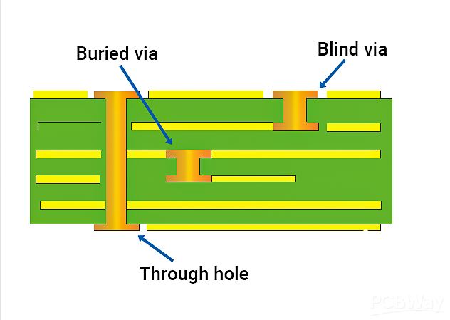
Blind vias: Through holes connecting outer and inner layers, extending only partially through the layers, not through the entire board.
Blind vias (BVHs)
Blind vias (BVHs) are a technique for connecting an outer layer of a PCB to an adjacent inner layer through a plated hole. Because the opposite side is not visible, they are called blind vias. This manufacturing process can improve the space utilization of PCB circuit layers. However, careful attention must be paid to the drilling depth (Z-axis), as this often makes plating inside the hole difficult, leading manufacturers to almost completely abandon this process. Alternatively, necessary connection holes can be drilled on individual circuit layers during the manufacturing process and then bonded together at the end. For example, in a 2+4+2-layer circuit board, the outermost two layers can be drilled first, or layers 2+4 can be drilled simultaneously, but this requires more precise positioning and alignment equipment. Consider the example of purchasing a building above. In a six-story building, only staircases connecting the first and second floors, or the fifth and sixth floors, are called blind vias.
Buried vias (BVHs) are located within the circuit board, connecting only inner layers without interfering with outer layers.
Buried vias (BVHs) connect two or more inner layers without reaching the outer layers. This process cannot be achieved with post-bonding drilling; the inner layers must be partially bonded first, followed by plating, before the final bonding is completed. Buried vias are more time-consuming and costly than plated through-holes or blind vias. They are commonly used on high-density PCBs (HDI) to increase available space for additional circuit layers. For example, if a six-story building only has a staircase connecting the third and fourth floors, it’s called a buried via. Buried vias are invisible on the board’s exterior and are located on inner layers.
IPC standards recommend that the diameter of blind and buried vias should not exceed 6 mils (150 μm).
The use of these two types of vias allows for more flexible routing in multilayer boards, which is particularly critical in scenarios such as BGA packaging, high-speed signal routing, and dense designs.
Why use blind and buried vias?
Increasing routing density
In high-layer PCBs, traditional through holes penetrate the entire board, occupying a significant amount of space. Blind/buried vias avoid occupying outer layer space, leaving more margin for surface routing.
Optimizing electrical performance
Reducing unnecessary hole wall capacitance and signal reflection paths helps improve the integrity of high-speed signal transmission.
Enhancing design flexibility
Enabling localized layered routing, simplifying stackup structures, and implementing complex functional layouts in space-constrained environments.
Reducing board thickness/improving structural strength
By replacing through holes, blind/buried vias can control board thickness to a certain extent, making products lighter and thinner while reducing areas of mechanical stress concentration.
Process challenges and the importance of selection
While blind and buried vias are very useful in design, their processing is significantly more challenging than conventional through holes. For example, controlling blind hole depth, drilling deviation, and filling with resin all place higher demands on the manufacturing process. Improper design or inadequate manufacturer process can easily lead to problems such as short circuits, open circuits, and board warping.
Therefore, when implementing blind/buried via designs, engineers typically prioritize PCB manufacturers with mature blind/buried via process experience.


0 Comments