




A blind via connects one outer PCB layer to an internal layer without reaching the opposite surface. A buried via connects internal layers only. Both can recover routing space that a through via would occupy, but their value depends on which layers need that space and whether the proposed connections fit a practical manufacturing sequence.
Start by writing down each connection’s start and end layer. Then compare a conventional through-via layout with the proposed blind/buried construction. A smaller hole or fewer layers does not automatically make the finished board cheaper, more reliable or electrically better.
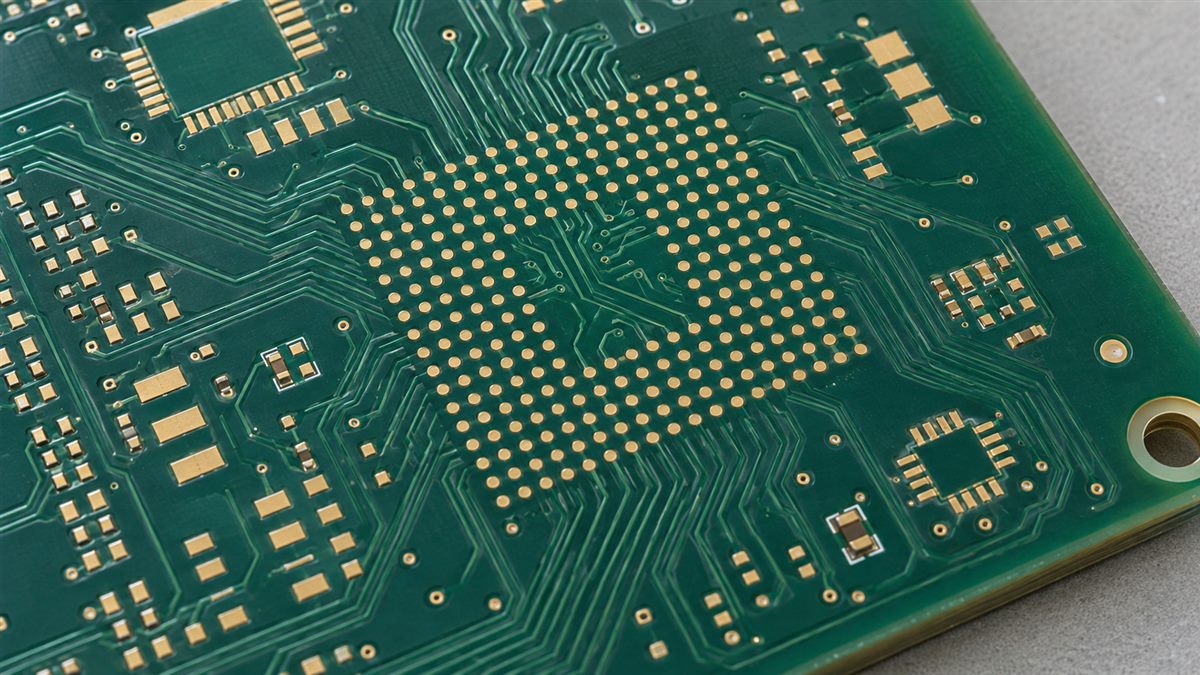
How Do Blind and Buried Vias Connect PCB Layers?
Classify the via by where its conductive structure begins and ends in the finished board, not by its color in the layout editor or whether you can see light through it. Copper plating makes the vertical connection; an ordinary unplated hole does not provide that connection.
| Structure | Physical span | Six-layer example | Space still occupied |
|---|---|---|---|
| Through via | Top to bottom | L1 to L6 | Hole and required clearances across the board |
| Blind via | One outer layer to an inner layer | L1 to L2, or L6 to L5 | Its actual span, including the outer-layer land |
| Buried via | Inner layer to inner layer | L2 to L5 | Its internal span; neither outer surface |
Physical span and electrical connection are different. A through via can pass through six layers while connecting copper on only L1 and L3. Clearances around its barrel on the other layers prevent unwanted contact. Those clearance openings still interrupt available routing or plane copper. They are often called antipads.
Likewise, a buried via spanning L2-L5 need not connect electrically to every intermediate layer. The artwork, pads and clearances decide that. A drill-pair label alone does not describe the complete net connection.
Blind/buried describes location. Microvia describes a particular small interconnect structure; via-in-pad describes placement in a component land. These are not mutually exclusive categories. A blind microvia can also be via-in-pad. See the broader PCB via types comparison for the other structures.
A Six-Layer Example: Which Space Does Each Via Free?
On a six-layer board, an L1-L2 blind via leaves L3-L6 free of that via’s barrel, while an L2-L5 buried via leaves L1 and L6 free. This is the useful distinction: a blind via does not free its own entry pad, and a buried via does not leave every internal layer unobstructed.
Imagine a hypothetical 1+4+1 construction: a four-layer L2-L5 core subassembly with one build-up layer added on each side. The following is a connection-planning example, not a production-ready stackup. Plane assignments, materials, dielectric thicknesses and permitted drill spans still require engineering approval.
| Connection required | Candidate structure | What it gains | What must still be checked |
|---|---|---|---|
| A: top component on L1 to routing on L2 | L1-L2 blind via | No barrel from this via in L3-L6 | Escape geometry, target pad, dielectric depth and return path |
| B: internal routing from L2 to L5 | L2-L5 buried via in the core | Both finished surfaces remain available | Clearance to unrelated copper on L3/L4; core drilling and plating route |
| C: top-to-bottom connection | L1-L6 through via | Simple full-thickness connection | Pad/plane clearances and unused electrical stub, if any |
For connection B, a trace on L1 can pass over the buried via’s location without contacting its barrel because dielectric separates them. That does not waive normal trace spacing or signal-coupling checks. On L3, however, the same via passes through the layer, so unrelated copper needs the specified clearance.
Now change connection A to L1-L3. It is still a blind connection if it does not reach L6, but it is not automatically the same manufacturing operation as L1-L2. A deeper controlled-depth hole, a qualified skip structure, or multiple shorter connections may be needed. Changing a dropdown in CAD does not settle that choice.
A useful self-check is to cover the via names and read only the endpoints: L1-L2 is outer-to-inner; L2-L5 is inner-to-inner; L1-L6 is outer-to-outer. Then mark the layers with actual copper contact separately. This prevents a common mistake: calling every internal connection a buried via even when its physical hole reaches a surface.
When Is the Extra Manufacturing Cost Worth It?
Use blind or buried vias when they solve a demonstrated routing, packaging or electrical problem that a simpler construction cannot solve acceptably. Do not add them merely to make the layout look advanced or to remove visible holes.
For a fine-pitch component, first test whether its pads, through-via lands and required clearances leave a usable escape channel. Package pitch alone is insufficient: the ball pattern, pad diameter, routing rules and number of signals all matter. If conventional fanout fits with margin, special vias may add cost without an equivalent benefit.
| Problem | Compare these options | Decision evidence |
|---|---|---|
| Through vias block escape routes | Placement/routing changes, additional layers, blind microvias | Actual routed breakout using approved pad and clearance rules |
| Surface space is needed above an internal connection | Reroute the internal net or use a buried span | Layer map showing exactly which surface area is recovered |
| A long unused via stub harms a high-speed channel | Different layer transitions, shorter vias, or backdrilling | Channel analysis including the transition and return path |
| Fewer board layers are proposed as a cost saving | Conventional multilayer versus HDI build at the same quantities | Two quotes including fabrication cycles, filling and qualification |
The main cost change can come from introducing a new drill/plating/lamination route, not simply from adding one more hole. Nevertheless, additional holes are not universally free: drilling time, density, fill requirements and yield can still matter. Ask which operation changes when a proposed layer pair is added.
Backdrilling removes unwanted copper from a plated through-hole stub. It does not remove the physical hole or restore routing space inside that drilled area. It can solve a signal-stub problem without solving a dense-placement problem. Similarly, a shorter signal via still needs a suitable return-current path; changing the via type alone cannot guarantee lower EMI.
Which Layer Pairs Can a Fabricator Actually Build?
A usable layer pair must be accessible at a viable drilling and plating stage, with geometry the fabricator can qualify. The final layer labels are only the starting point; the build sequence determines how that connection can exist.
In the six-layer example, an L2-L5 connection can be drilled and plated while that core subassembly is still exposed. Adding the outside build-up layers makes it buried. An outer blind connection may then be created through the added dielectric to its target land. Other constructions use different subassemblies or drilling routes.
Watch for crossing spans, such as an L1-L3 blind connection combined with an L2-L4 buried connection. Those spans overlap without one being fully contained inside the other. They may not fit a simple sublamination sequence. Do not declare them impossible in every technology, but do not route the board around them before the fabricator approves the complete combination. Multi-CB’s design guidance specifically warns that overlapping spans can increase cost.
Request a marked stackup showing the approved via structures together. An approval for one L1-L3 hole and a separate approval for one L2-L4 hole are not necessarily approval to combine both in the same build. Consolidating several requested spans into fewer qualified layer pairs may reduce complexity, but only if the electrical routing still works.
For the detailed drilling, cleaning and metallization sequence, use the separate blind via fabrication process guide. Keep the layer-pair approval attached to the drawing revision so a later stackup change cannot silently invalidate it.
How Do You Check Via Depth, Pads and Filling?
Check the actual via depth against the relevant hole diameter, then review the target land, clearance and filling requirements as a group. Total board thickness is not the correct depth for a short L1-L2 blind via.
For the following teaching examples, define aspect ratio = via depth / hole diameter. Suppliers may publish the inverse convention or distinguish drill diameter, finished hole diameter, and a laser hole’s entry/bottom diameters. Establish which dimensions their rule uses before comparing numbers.
- Example 1: a proposed 0.08 mm depth divided by a 0.10 mm reference hole diameter gives 0.8:1.
- Example 2: increasing depth to 0.16 mm while keeping that diameter gives 1.6:1.
The second cavity is twice as deep relative to its opening. Reaching and plating its bottom can be more demanding. Neither result is an automatic pass or fail: these are arithmetic examples, not PCBtry capability limits. Use the approved material, hole geometry and qualified process rule to decide whether to enlarge the hole, reduce the dielectric depth or change the connection structure.
The target land is the copper area the via must meet. A nominally centered CAD hole can still miss an adequate copper connection if drill registration and layer movement consume the available margin. Review the fabricator’s required land, annular connection and copper clearance, including tolerances, rather than checking only the drawn hole.
Filling is a separate requirement. A via under a solderable component pad may need filling, planarization and capping to control solder loss and surface flatness. A stacked microvia needs a qualified supporting structure beneath it. Solder-mask tenting is not equivalent to filling and copper capping. State the required finish instead of writing only “via-in-pad.”
There is no sound basis for imposing a universal 6 mil maximum on every blind and buried via merely from those names. They describe layer connectivity, not one diameter. Confirm the applicable structure definition and manufacturing rule instead of copying a dimension from a generic article.
How Can Hidden Connections Be Verified?
Verify both the intended net connections and the suitability of the physical interconnect. Electrical test, sectioning and thermal testing answer different questions; passing one does not prove all the others.
- Continuity/isolation test: checks the specified electrical network at the test conditions. It can reveal an open or short but does not show the copper interface.
- Representative microsection: exposes sampled geometry, copper coverage and interfaces. It is destructive and does not inspect every via or prove service life.
- Appropriate X-ray inspection: can help investigate some alignment or fill anomalies. Overlapping copper and resolution limit what it can establish.
- Agreed thermal exposure with resistance monitoring: can reveal connections that become unstable under assembly-like or service-related stress. Coupon design, conditions and acceptance limits must match the intended evaluation.
For example, if a net passes bare-board test but becomes intermittent after reflow, the investigation should consider a weak via interface or other assembly-related damage, not assume the original netlist was wrong. Record when the fault appears, temperature dependence, affected nets and board revision before destructive analysis.
IPC’s 2019 microvia reliability warning describes failures that escaped traditional acceptance inspection and emphasizes performance-based testing. It is a reason to agree appropriate evidence for demanding microvia builds, not a claim that every stacked via will fail. A photograph of a good-looking board cannot replace that evidence.

What Must Be in the Drill-Pair Handoff Package?
Send a layer-pair schedule that matches the released stackup, drill data and net intent. The recipient should be able to identify every special via without guessing from filenames or a screenshot.
Step 1: Freeze the layer names. Number copper layers consistently from top to bottom. Match CAD names to fabrication drawing names and identify the approved stackup revision.
Step 2: List every distinct span. For each via structure, record an identifier, start/end layer, electrically connected layers or net reference, hole-size convention, pad requirements and fill/cap treatment. Include ordinary through vias so the special files cannot be mistaken for the complete drill set.
Step 3: Export and reopen the manufacturing data. Review the actual released outputs, not only the editable board. Check each blind/buried drill pair against its start/end layers and distinguish plated from non-plated holes. Altium’s official via documentation explains separate microvia drill-pair outputs; the exact export controls depend on the CAD tool and version.
Step 4: Check a known connection in each structure. Trace one intended net from its component pad to the destination layer. Confirm copper contact where required and clearance where not required. Include the signal return path in high-speed reviews.
Step 5: Close the engineering questions. Obtain the approved combined layer-pair map, process assumptions and test scope before release. Mark each unresolved item as pending; a quotation alone is not necessarily technical approval.
A reusable handoff record can use these fields:
- Board/revision; stackup/revision; top-to-bottom layer-name map.
- Via ID; start layer; end layer; net/connectivity reference; drill-file name.
- Depth and diameter definitions; pad/clearance requirements; fill/cap requirement.
- Supplier-approved construction; open DFM questions; approval date/revision.
- Quantities; acceptance requirements; electrical test and agreed coupon evidence.
If a file calls an L2-L5 buried structure “through,” stop and resolve the mapping rather than relying on the filename alone. This is precisely the kind of mismatch that can survive a visually tidy CAD layout.
Blind and Buried Via Questions Before Layout Release
Can a two-layer PCB have a buried via?
Not in the usual finished-board definition: a two-layer board has no pair of internal copper layers to connect. A normal plated connection between its top and bottom copper is a through via. Do not confuse a covered or plugged through hole with a buried via; covering changes the opening, not its layer span.
Does a blind via have to stop at the immediately adjacent layer?
No. The name only requires an outer-to-inner connection that does not reach the opposite surface. A deeper span needs a compatible construction and drilling/plating route. Check the entire set of layer pairs, not just one hole in isolation. A skip microvia and multiple stacked microvias are also different structures, even if they reach the same destination layer.
Can blind and buried vias be used on the same board?
Yes, and through vias may be present too. The six-layer example combines all three. What matters is whether the complete stackup can be manufactured with the proposed spans, pads, materials and process sequence. Send the combined map for approval; independently acceptable structures can create extra complexity when used together.
Are buried vias always more expensive than blind vias?
No fixed ordering applies to every board. A buried hole made in an existing core process can have a different cost effect from a blind structure requiring extra build-up, fill or qualification. Compare complete builds at the same quantity and acceptance requirements. Ask which new operation each proposed structure introduces.
Are stacked microvias always better than staggered microvias?
No. Stacking can save lateral routing space, while staggering needs an offset connection and more area. Stacking also makes the connection depend on the filled structure and interface below it. Select the arrangement against routing needs and the supplier’s qualified reliability evidence, not an assumption that the smallest footprint is automatically the best design.
Will a buried via prevent component placement above it?
The buried via itself does not emerge on the finished surface, so it does not require an exposed outer-layer via land there. Component placement still has to meet normal assembly, thermal, mechanical and electrical rules. Conversely, a blind via starts at one outer surface and may need a specified fill/cap treatment if placed in a solder pad.
Does a 3D CAD view prove the board can be built?
No. It helps you inspect intended spans and spot an obvious setup mistake, but it does not validate the factory’s process sequence, plating capability or registration margin. Use the view alongside manufacturing outputs and the approved stackup. Old tutorial menus may also differ from the version of the CAD tool you use.
Can a buried via be repaired after fabrication?
Its internal location makes direct access difficult, and repair may be impractical or unacceptable for the product. An accessible external wire modification is not equivalent to restoring the original internal construction. Investigate the failure with the fabricator and define disposition under the product’s quality requirements rather than assuming an internal defect can be patched later.
Ready for a fabrication review? For a project considering HDI PCB manufacturing, send the stackup, layer-pair schedule, Gerber or ODB++ data, drill files, quantities and fill/test requirements to sales@pcbtry.com or through the contact page. Ask for confirmation of the combined via construction and a comparison with a simpler alternative where feasible.



1 Comment
PCB Blind Via Fabrication Process: Drilling, Plating and DFM Checks - thindry pcb manufacturer · 08/27/2026 at 11:10
[…] “Blind via” describes where a via starts and ends; it does not define one universal hole size or drilling method. A laser-drilled microvia is often blind, but a larger controlled-depth mechanical hole can also be blind. The approved stack-up, via depth, diameter, material system and reliability class determine the route. For a broader comparison of structures, see blind and buried vias in PCBs. […]