
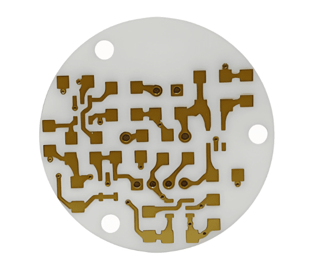
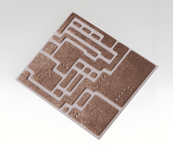
What Is Ceramic PCB?
A ceramic PCB is a circuit board that uses ceramic materials as its base instead of traditional FR4. These materials include alumina, aluminum nitride, and others. The ceramic base provides excellent thermal conductivity, high insulation, and strong mechanical strength. Ceramic PCBs are often used in industries where heat resistance and reliability matter most.
Unlike standard boards, ceramic PCBs allow direct copper bonding without using adhesives. This feature improves heat transfer and performance. These boards are ideal for power electronics, LEDs, and aerospace applications where reliability under stress is a must.
Types of Ceramic PCB
Ceramic PCBs come in several variations depending on their manufacturing methods and materials. Each type is designed for specific applications, and choosing the right one can greatly impact a project’s success.
1. Thick Film Ceramic PCB
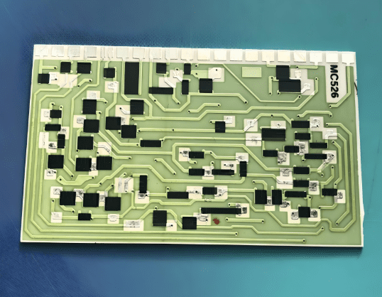
Thick film ceramic PCBs are created by screen-printing conductive, resistive, and dielectric pastes onto a ceramic substrate, typically alumina. The printed layers are then fired at high temperatures to cure and bond the materials. These boards are widely used in medical devices, automotive sensors, and consumer electronics where compactness and reliability are important. Thick film boards support multi-layer circuit designs, allowing integration of resistors and capacitors directly onto the surface.
2. Thin Film Ceramic PCB
Thin film ceramic PCBs are manufactured using sputtering or vacuum deposition methods, which apply very fine layers of conductive materials on a ceramic surface. These boards are ideal for applications that require extreme precision and fine line geometries, such as micro-electromechanical systems (MEMS), sensors, and high-frequency components.
Although they offer high precision and performance, thin film ceramic PCBs are costly and primarily used in specialized applications.
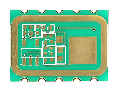
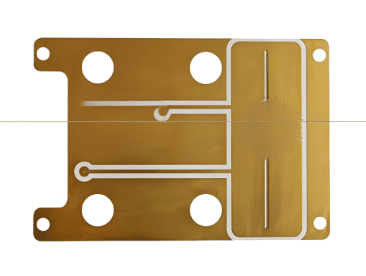
3. Direct Bonded Copper (DBC) Ceramic PCB
DBC ceramic PCBs are made by bonding a layer of copper directly to a ceramic substrate—usually alumina (Al₂O₃) or aluminum nitride (AlN)—through a high-temperature oxidation process. This process forms a strong, thermally conductive connection between the copper and the ceramic, making these boards ideal for power modules and high-current circuits.
DBC PCBs are commonly used in IGBT modules, LED lighting, automotive power controllers, and industrial automation systems.
4. Active Metal Brazed (AMB) Ceramic PCB
AMB PCBs are created by brazing metal—typically copper—to a ceramic base using active metals like titanium. This type of bonding produces excellent adhesion and thermal performance, making AMB boards suitable for very high-power applications.
AMB ceramic PCBs are often found in electric vehicle control units, renewable energy systems, and aerospace-grade electronic devices.
Features of Ceramic PCB
- High thermal conductivity
- Excellent electrical insulation
- High mechanical strength
- Compact and dense layouts
- Chemical and moisture resistance
- Stability in extreme conditions
- Long lifespan
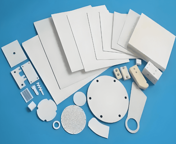
What Materials Are Used in Ceramic PCB?
Ceramic PCB materials play a huge role in determining the board’s performance. The most common ones include:
1. Alumina (Al₂O₃)
Alumina is the most common ceramic substrate, offering a good balance of performance and affordability. It has thermal conductivity in the range of 15–35 W/mK, good insulation, and reliable mechanical properties. It’s widely used in LED lighting, sensors, and automotive components.
2. Aluminum Nitride (AlN)
AlN provides much higher thermal conductivity—typically 170–200 W/mK—and maintains good electrical insulation. It’s excellent for high-power applications like laser diodes, RF amplifiers, and industrial motor drivers. Though more expensive than alumina, AlN delivers better heat dissipation.
3. Beryllium Oxide (BeO)
BeO offers thermal conductivity over 250 W/mK, but it’s rarely used due to its toxic nature during processing. When safety protocols are followed, BeO is used in military, aerospace, and advanced communication systems.
4. Zirconia (ZrO₂)
Zirconia has lower thermal conductivity but exceptional mechanical toughness. It is sometimes used in biomedical sensors, optical applications, and structural ceramic parts.
Each material comes with trade-offs. For most industrial applications, alumina is sufficient, while AlN is preferred for more heat-sensitive or performance-critical projects.
Ceramic PCB vs FR4 PCB: What’s the Difference?
When it comes to Ceramic PCB vs FR4, each has its own strengths. FR4 PCBs are cost-effective and widely used in mass-market products. Ceramic PCBs, on the other hand, are ideal for advanced applications where performance, thermal control, and durability are essential. Here’s a detailed comparison between them:
| Feature | Ceramic PCB | FR4 PCB |
| Base Material | Inorganic ceramics (Alumina, AlN, BeO, Zirconia) | Epoxy resin reinforced with woven fiberglass (FR4) |
| Thermal Conductivity | Very high (15–200+ W/m·K depending on material) | Low (~0.3–0.4 W/m·K) |
| Electrical Insulation | Excellent (even at high temperatures) | Good, but can degrade at high temps or humidity |
| Heat Dissipation | Efficient, ideal for power and LED applications | Poor, often requires heat sinks or metal cores |
| Thermal Expansion (CTE) | Low and close to semiconductors (5–9 ppm/°C) | High (14–17 ppm/°C), mismatched with chips |
| High-Temperature Resistance | Excellent (can withstand >800°C in some cases) | Limited (typically max 130–180°C) |
| Dielectric Constant (Dk) | Low and stable over temperature/frequency | Higher and less stable, varies with resin and filler |
| Mechanical Strength | High hardness but brittle (risk of cracking under stress) | More flexible, less brittle, better for dynamic environments |
| Moisture Absorption | Very low (near zero) | Moderate (can swell and lose insulation over time) |
| Design Precision | High—supports fine pitch, small trace width/spacing | Moderate—standard resolution is limited by fiberglass weave |
| Layer Count | Usually 1–2 layers; multilayer possible but expensive | Supports multilayer (4, 6, 8, or more) easily |
| Copper Bonding | Direct bonding (DBC, AMB), no adhesive layers | Copper is etched from laminate bonded with epoxy |
| Processing Complexity | Requires special tools, processes like laser cutting or brazing | Standard PCB equipment works for FR4 |
| Size Limitations | Smaller max panel sizes due to material fragility | Large panel sizes possible |
| Cost | Higher (materials + processing) | Lower (mass production friendly) |
| Typical Applications | Power modules, high-brightness LEDs, RF/microwave, medical, aerospace | Consumer electronics, IoT, industrial controllers, general devices |
| Environmental Resistance | Excellent (corrosion, humidity, chemicals) | Moderate; needs coating for harsh environments |
| Weight | Denser material, slightly heavier per unit | Lightweight |
| Reworkability | Limited; brittle nature makes rework tricky | Easier to drill, cut, or modify during prototyping |
| Signal Integrity | Better for high-speed and high-frequency circuits | Acceptable for most standard-speed applications |
Ceramic PCBs outperform FR4 in demanding situations, especially in power and high-frequency systems. FR4, on the other hand, is more cost-effective and suitable for low to mid-range electronics.
Considerations When Designing a Ceramic PCB
Designing a ceramic PCB involves different challenges than working with FR4. Here are key factors to keep in mind:
1. Material Selection
Your choice between alumina, aluminum nitride, or other ceramics should match the needs of your application. For heat-intensive systems, AlN is often the best option.
2. Copper Thickness
Depending on the current load, thicker copper layers may be needed. DBC and AMB processes allow for copper thicknesses up to 300 μm or more.
3. Component Placement
Ceramic boards offer limited flexibility compared to FR4. Ensure your components are placed carefully to avoid design rework.
4. Thermal Management
Use thermal vias, heat sinks, or integrated cooling structures to further enhance heat dissipation.
5. Mechanical Mounting
Ceramic substrates are hard but brittle. Proper mounting methods and housing design help reduce mechanical stress during operation.
6. Surface Finish and Soldering
Choose finishes like ENIG or OSP that are compatible with your assembly methods. Reflow soldering works, but temperature settings must be carefully controlled to avoid damage.
Designing ceramic PCBs with these points in mind ensures smoother production and fewer failures in the field.
What Are Ceramic PCBs Used For?
Ceramic PCBs support a wide range of industries. Their excellent properties make them ideal for:
1. Power electronics
Ceramic boards handle high voltages and strong currents. They are used in inverters, converters, and motor drives.
2. LED lighting
High thermal conductivity allows LEDs to last longer and shine brighter. Ceramic substrates are common in high-power lighting systems.
3. RF and microwave systems
Ceramic PCBs have low dielectric loss, making them suitable for antennas, transceivers, and radar equipment.
4. Medical devices
They support precision and reliability, especially in implants and diagnostic equipment.
5. Automotive and aerospace
Ceramic PCBs handle vibration, heat, and pressure. They are found in engine control units, sensors, and avionics.
6. Laser and sensor technology
Stable electrical properties and excellent heat resistance make them ideal for sensitive sensors and laser diodes.

Your Best Ceramic PCB Manufacturer: Thindry Circuits
When performance matters, choosing the right ceramic PCB manufacturer is key. That’s where Thindry circuit comes in.
We specialize in manufacturing ceramic PCBs using materials like alumina, aluminum nitride, and zirconia, based on your project’s thermal and electrical needs. Whether you need a simple prototype or large production batches, we’re equipped to support you at every stage. Here’s why engineers and buyers choose us:
- Rigorous quality control: Every board is inspected using advanced testing tools.
- Flexible prototyping and mass production: From quick-turn samples to full-scale runs.
- Professional support: Our engineers guide you through every stage—from material selection to final delivery.
- Data traceability available: Every PCB has a traceable manufacturing record for safety and compliance.
Our ceramic PCBs are already powering products in over 80 countries. If you need custom ceramic PCBs that perform under pressure, we’re here to help. Contact us today for a quote or free consultation.
FAQs
1. What’s the typical thickness of a ceramic PCB?
It ranges from 0.25 mm to 2.0 mm depending on the material and application. Commonly used thickness is 0.635 mm or 1.0 mm.
2. Can ceramic PCBs be multilayer?
Yes, multilayer ceramic PCBs are available. However, they are more complex to fabricate and more expensive than single-layer boards.
3. How do I choose between alumina and aluminum nitride?
If you need better heat dissipation, go with AlN. For cost-sensitive applications with moderate thermal needs, alumina works well.
4. What’s the minimum line width/spacing for ceramic PCBs?
Depending on the process, the minimum line width and spacing can reach 0.1 mm (4 mil) for high-precision thick film ceramic PCBs.
5. Are ceramic PCBs safe for medical devices?
Yes. Ceramic PCBs meet strict standards and are commonly used in medical instruments, especially those that need reliable performance over time.

0 Comments