Blog
CCTV PCB Manufacturing Process: Design, Assembly and Testing
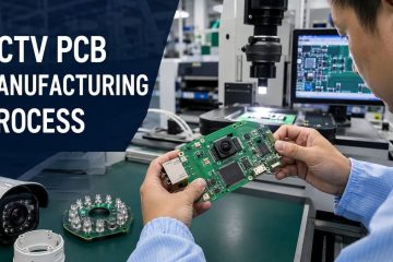
Follow the CCTV PCB manufacturing process from DFM and bare-board fabrication through SMT assembly, programming, image testing and final release.



Follow the CCTV PCB manufacturing process from DFM and bare-board fabrication through SMT assembly, programming, image testing and final release.
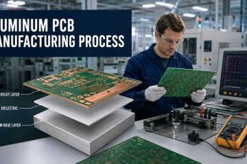
Follow the aluminum PCB manufacturing process from DFM and IMS material preparation through circuit imaging, bonding, machining, finishing and final testing.
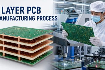
Follow the 4 layer PCB manufacturing process from DFM and inner-layer imaging through lamination, plating, inspection and electrical testing.
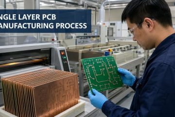
Follow the single layer PCB manufacturing process from DFM and copper imaging through etching, drilling, solder mask, finish and electrical testing.
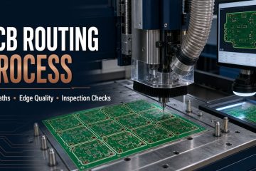
See how PCB CNC routing controls profile data, toolpaths, fixtures, tabs, edge quality, depaneling and dimensional inspection.
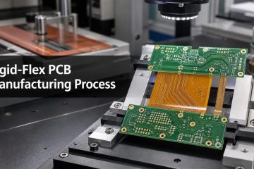
See how rigid-flex PCBs are built, which process controls prevent transition and plating failures, and what test evidence to request before ordering.
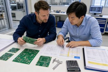
Estimate PCB cost by defining bare board versus PCBA scope, then compare quantity, materials, layer count, finish, testing, tooling and delivery on one RFQ.
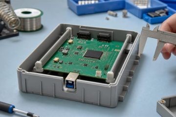
Compare rails, edge clips, adhesive standoffs and controlled bonding for mounting a PCB without holes while protecting clearance, serviceability and board stress.
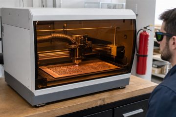
Learn how to make a prototype PCB with a laser engraver using an etch-mask workflow, calibration grid, inspection checks and realistic process limits.
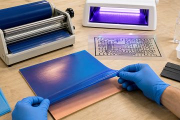
Learn how to apply PCB dry film photoresist, calibrate UV exposure, develop a clean pattern, diagnose defects and prepare files for fabrication.
If you have any enquiry about quotation or cooperation, please feel free to email us at sales@pcbtry.com or use the following enquiry form. Oursales representative will contact you within 24 hours. Thank you for your interest in our products.