




DFM and DFA in PCB manufacturing check whether a design can be fabricated and assembled using the intended production processes. In a practical PCB review, DFM focuses on the bare board, while DFA focuses on installing and soldering its components. A board can pass the first review and still fail the second: the copper and holes may be manufacturable, but a connector may block a placement tool or an open via may draw solder away from a joint.
Use the distinction to assign checks, not to divide responsibility. Fabrication, assembly and design engineers need to agree on the same files, process assumptions and unresolved issues before production begins.
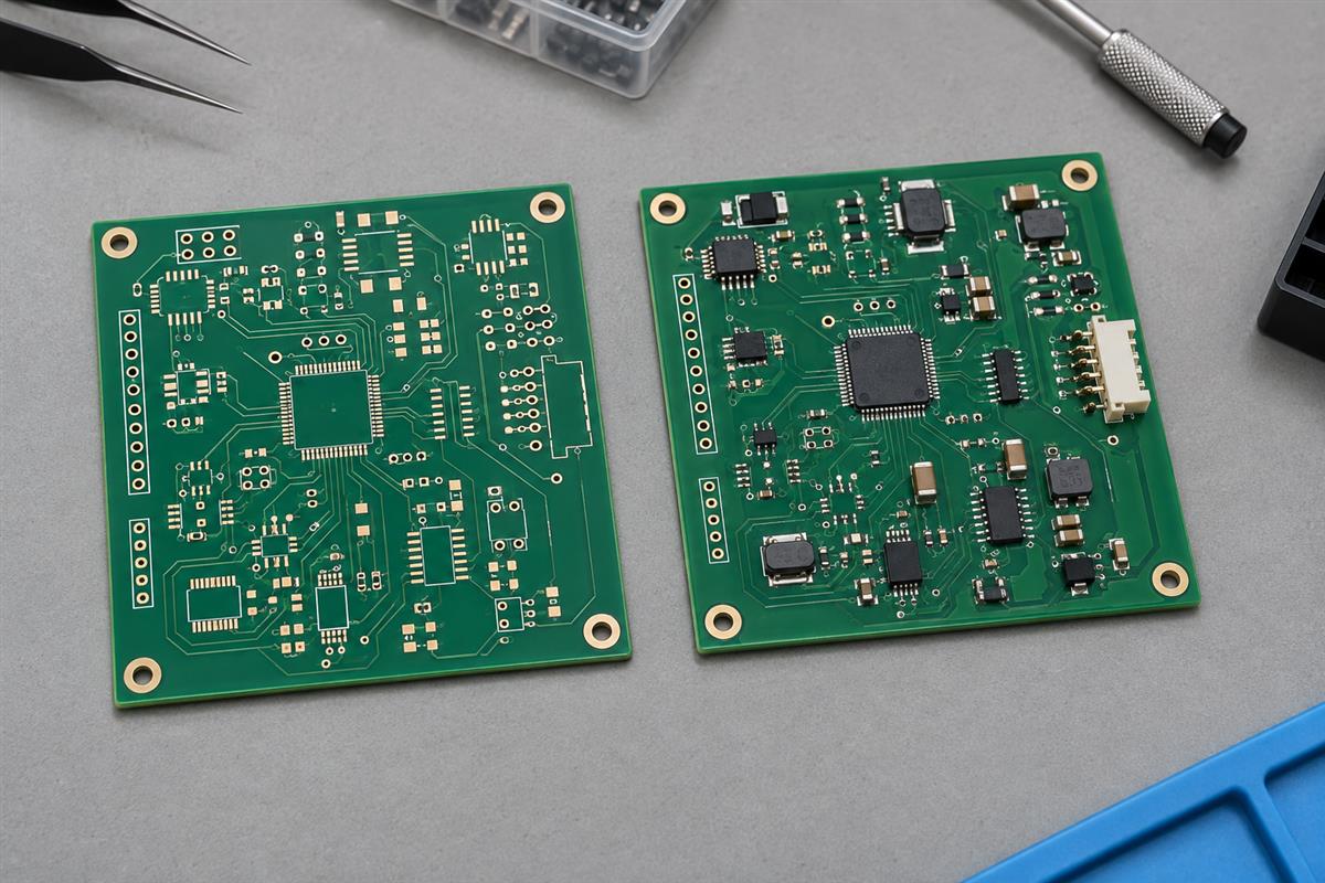
DFM vs DFA: Which Problem Does Each Review Solve?
DFM means design for manufacturing or manufacturability. DFA means design for assembly. Think of DFM as asking, “Can the factory make this board construction?” and DFA as asking, “Can the assembly line populate, solder and handle it correctly?” Some suppliers use DFM as an umbrella term that includes assembly checks. Ask what their review actually covers instead of relying on the label.
| Review | Typical question | Useful output |
|---|---|---|
| Fabrication DFM | Can this copper geometry, hole structure and stackup be made with the quoted process? | Confirmed construction and a list of fabrication changes or exceptions |
| Assembly DFA | Do the specified parts fit the footprints, and can the planned line place and solder them? | Resolved footprint, orientation, access and assembly-data issues |
| Design for test, often called DFT | Can the required signals be accessed and the intended defects detected? | Agreed test access, fixtures and coverage limitations |
| Electrical and product validation | Does the assembled product meet its functional and environmental requirements? | Results against the product’s test and qualification plan |
These reviews support each other but are not interchangeable. A manufacturable board is not automatically electrically correct, safe or reliable in service. Likewise, a clean CAD design-rule check only demonstrates compliance with the rules that were configured; it does not prove that the factory uses those same limits.
What Should a PCB Fabrication DFM Review Check?
A fabrication review should compare the released board data against the selected supplier’s capability for the actual stackup, materials and copper thickness. Do not copy a minimum trace width or hole size from an unrelated board and treat it as universal.
| Check | What can go wrong? | What to confirm |
|---|---|---|
| Copper width and spacing | Fine features may be unsuitable for the required copper thickness or etching route. | Layer-specific geometry and the fabricator’s accepted production limits |
| Holes, slots and annular rings | Confusing drill size with finished hole size can cause fit or plating problems. | Finished sizes and tolerances, plated/non-plated definitions, drill spans and pad geometry |
| Stackup and materials | A quoted construction may differ from the one assumed in impedance calculations. | Layer order, material requirements, dielectric construction, copper and impedance targets where needed |
| Mask and legend | Registration limits may affect mask openings; legend can obscure exposed pads or markings. | Mask clearances and dams within the chosen process, plus readable assembly identification |
| Outline, routing and panel features | Ambiguous edges or slots can change fit, tooling or separation. | A single board outline, mechanical tolerances and an agreed panel/depaneling plan |
Example: a designer specifies a 0.30 mm finished plated hole, but the fabrication note only says “0.30 mm drill.” Those are not equivalent instructions. The review must establish the finished requirement and let the fabricator select a compatible production drill and plating allowance. Do not silently enlarge a connector hole or reduce an annular ring to make a warning disappear.
Ask the supplier to identify the affected layer, coordinate or feature and the proposed change. A message saying “DFM failed” is not enough to approve a correction. Keep electrical requirements separate from production convenience: a wider trace or different stackup may be easier to manufacture but still needs design approval if it changes impedance, clearance or mechanical fit.
What Should a PCB Assembly DFA Review Check?
DFA should verify the relationship between the actual component, its land pattern, placement data and the intended soldering process. Checking component spacing alone misses wrong packages, polarity conflicts and inconsistent files.
- Part and footprint: match the full manufacturer part number to the package drawing, pin numbering, pitch, exposed pad and height. A family name is not enough when several package options exist.
- Orientation: reconcile the datasheet, pin-1 or polarity marking, assembly drawing and placement preview. A rotation value is meaningful only within the agreed coordinate convention.
- Physical access: check component bodies and leads, not just pad centers. Include placement, connector mating, inspection and rework access where required.
- Soldering: review land patterns, paste openings, thermal connections, accessible joints and mixed SMT/through-hole operations with the assembler.
- Handling: establish usable board edges, support, tooling and fiducials for the selected line. Overhanging connectors or underside components can affect fixtures.
- Build variant: reconcile populated and do-not-populate locations so the BOM, drawing and placement instructions describe the same assembly.
The Eurocircuits BOM and CPL guidance illustrates the distinction: the BOM identifies parts and reference designators; placement data specifies location, side and rotation. Neither file alone defines the complete build.
For spacing, use a manufacturing courtyard: the reserved area around a component that accounts for the physical part and required process access. Eurocircuits describes this boundary and its rework role, but its published clearances are supplier-specific. Obtain limits appropriate to your package sizes, component heights and assembly process.
Fiducials are copper targets used to register the board or panel with production equipment. Their size, quantity, placement and clear area should be agreed with the assembler. See the fiducial guidance for a concrete supplier example, not a universal acceptance rule.
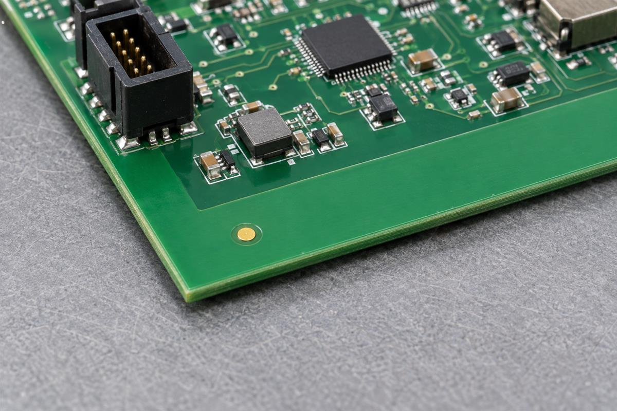
Where DFM and DFA Decisions Overlap
The most useful joint review covers features that are acceptable to one process but risky for another. Resolve these conflicts before either team treats the design as approved.
Thermal vias can affect solder attachment
A plated via under an exposed thermal pad may provide a useful heat path and still allow solder to wick into the hole during reflow. The solution depends on the package, via construction, mask and paste design. Filling and capping, different via locations or another validated process may be appropriate; do not assume that every via-in-pad arrangement is wrong or that all tenting methods are equivalent.
Texas Instruments’ PowerPAD application report explains the relationship between thermal lands, vias and solder attachment for that package technology. Use the exact device datasheet and an agreed assembly process for dimensions. The joint review should answer: what via construction is being ordered, how is solder loss controlled, and how will the joint be evaluated?
A panel can be routable but difficult to assemble
A board outline may be straightforward to route while leaving no usable edge for a conveyor. A connector may fit the enclosure but overhang a rail, or a breakaway tab may be too close to a sensitive component for the proposed separation method. Fabrication and assembly should review the panel drawing together, including support and depaneling. Changing the panel is not merely an efficiency decision if it changes mechanical stress or access.
A footprint can be connected but physically wrong
Consider a hypothetical replacement component with the same electrical pin functions but a different body width. The netlist can remain correct and DRC can show no copper violation, yet the part may collide with its neighbor or need a different land pattern. A purchasing substitution therefore needs package and process review, not just an electrical comparison.
How to Close Review Findings Before Production
Close a finding only when the design owner and the relevant supplier agree on a documented disposition and the released files contain that decision. A passed report from an earlier revision is not approval for the current build.
Step 1: Fix the scope and revision
Identify the board and assembly revisions, quantity, fabrication construction, assembly route and test scope. Separate a prototype feasibility question from production acceptance. Make clear which files the reviewer is evaluating.
Step 2: Review the exported package
Open the actual fabrication outputs, overlay the drills and outline, and compare assembly files against the same revision. Native CAD views alone cannot show an omitted output layer or a placement file exported before the final change.
Step 3: Record each issue with an owner
Give each finding a location, requirement, consequence and proposed action. Distinguish a missing instruction from a feature outside capability. Missing information needs clarification; a geometry problem may need a design change or a different process.
| Example finding | Owner and action | Evidence needed to close |
|---|---|---|
| Unspecified treatment of vias in U1’s thermal pad | Designer, fabricator and assembler agree on construction and soldering approach. | Updated fabrication note and matching assembly review disposition |
| Connector pin 1 conflicts with the placement preview | Designer checks the exact datasheet and corrects the drawing or placement output. | Re-exported files and a reviewed orientation preview |
| Small component obstructs a planned test probe | Design and test owners agree on access or an alternative test method. | Revised access geometry or documented coverage limitation |
| Two different board outlines appear in the archive | Release owner removes ambiguity and regenerates the package. | One authoritative revision checked in an independent viewer |
Step 4: Approve changes and controlled exceptions
Correct the design and re-export affected files when possible. If an exception is accepted, record its scope, reason, responsible approver and any inspection or build restrictions. “The supplier said it is probably fine” is not an acceptance criterion. A supplier cannot waive the customer’s electrical or product-safety requirements.
Step 5: Recheck and release one package
Re-run affected checks after changes, verify cross-file consistency and obtain agreement on the release revision. If a later substitution, stackup change or panel change affects the reviewed assumptions, reopen the relevant review. Keep prototype build feedback linked to the issue log; a successful first unit does not prove every production risk has disappeared.
What to Send for a DFM and DFA Review
Send one controlled package that tells the reviewer what to fabricate, what to assemble and which requirements cannot be changed without approval. Ask which data formats the supplier accepts before exporting.
- Fabrication layer data and drill files, or another explicitly accepted manufacturing format
- Board outline, stackup, material/copper/finish requirements and critical tolerances
- Special requirements such as controlled impedance, via treatment or specified acceptance criteria
- BOM with manufacturer part numbers, quantities, reference designators and approved substitution policy
- Placement data, assembly drawing, polarity information and do-not-populate instructions
- Panel and mechanical constraints, including overhangs, keep-outs and mating access
- Programming and test requirements, plus known risks or unresolved questions
- Revision identifier, intended quantity and the person authorized to approve changes
Do not put several obsolete releases into the same production archive. Eurocircuits’ input-data guidance explains why ambiguous versions make automated and manual interpretation unreliable. The broader lesson is to make the current manufacturing instruction unambiguous, whatever accepted format is used.
For PCB assembly review and quotation, send PCBtry the relevant files, quantity and known concerns through the contact page. Request a list of findings with proposed actions and the revision reviewed, so that a quote and an engineering approval are not mistaken for the same thing.
Frequently Asked Questions
Is DFA included in DFM?
Sometimes. Suppliers may use DFM broadly, while others separate bare-board DFM from assembly DFA. Ask whether the service checks footprints, BOM/placement consistency, soldering constraints and tooling access, rather than assuming these are included.
Can a bare PCB pass DFM and fail assembly?
Yes. The board may be fabricable while the specified part does not fit its footprint, a polarity instruction is contradictory or assembly tooling cannot reach the intended location. Fabrication approval alone does not resolve those problems.
Does a clean DRC report replace a supplier review?
No. DRC evaluates configured rules and available design data. It may not capture the selected supplier’s process restrictions, assembly equipment or missing manufacturing instructions. Use it as input to the review, not as final production approval.
When should DFM and DFA start?
Start before critical stackup and placement decisions are fixed. Review again on the final exported package. Waiting until procurement leaves less room to resolve construction, footprint or tooling problems without delay.
Are component clearances the same at every assembler?
No. Packages, component heights, placement tools, soldering route and rework requirements affect acceptable spacing. Obtain the chosen assembler’s requirements and check them against actual component boundaries.
Are thermal vias in an exposed pad always unacceptable?
No. They can be part of a valid thermal design. Their construction and the soldering process must control solder loss and joint formation. Follow device-specific guidance and agree on the implementation with both fabricator and assembler.
Does a DFM approval guarantee product reliability?
No. It addresses the reviewed manufacturing constraints. Functional testing, environmental qualification, electrical safety and reliability assessment remain separate obligations defined by the product and application.
What changes require another review?
Changes to the package, footprint, stackup, copper, via treatment, panel, assembly route or test access can invalidate previous assumptions. Reopen affected checks and confirm that all released files carry the approved revision.



3 Comments
Industrial PCB Manufacturing Process: Controls, Testing and Supplier Checks - thindry pcb manufacturer · 09/08/2026 at 06:16
[…] formal DFM review should identify values outside the chosen factory’s process window before tooling. The […]
PCB Design Process: Requirements, Layout and Release Checks - thindry pcb manufacturer · 09/08/2026 at 06:42
[…] reviewed capability instead of copying “standard” values from an unrelated board. The DFM and DFA review should resolve exceptions before […]
Bare PCB Manufacturing Process: Fabrication Steps, Controls and Final Testing - thindry pcb manufacturer · 09/08/2026 at 09:35
[…] drill, stack-up, and drawing must be resolved rather than guessed. See the practical role of PCB DFM review before production […]