
Introduction
In modern electronics, nearly every device—such as smartphones, computers, televisions, and microwave ovens—utilizes a PCB. So, what does PCB stand for? Why is it so crucial for the proper functioning of electronic devices? This article will detail the meaning of PCB, explain what a PCB is, list common board types, and describe how these boards operate. Whether you are an electronics engineer or a beginner, understanding what a PCB is, its constituent materials, and its fundamentals is essential.
What PCB Stands For
PCB stands for Printed Circuit Board. It is a flat, thin plastic board with integrated electronic components. A PCB includes an insulating substrate, copper foil connection traces, and solder pads for attaching electronic components. Serving the dual function of conductive pathways and an insulating base, it replaces complex wiring to achieve circuit connections between components.
The PCB is the mainboard for electronic components. Before the advent of printed circuit boards, electronic components were connected directly with wires, often resulting in messy and error-prone layouts. Nowadays, by using printed circuit boards, electronic devices avoid the errors associated with manual wiring. Components can be automatically installed via DIP or SMT, automatically soldered, and automatically tested, ensuring quality, enhancing productivity, reducing costs, and facilitating maintenance.
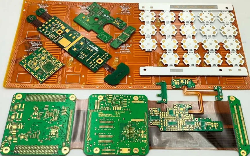
What Are the Types of PCB?
- Single-Sided PCB
This type of PCB has conductive material on only one side of the board for component connections. Composed of conductive material, layers, and a solder mask, single-sided PCBs are used in many complex devices such as printing equipment, speakers, and various everyday digital products. - Double-Sided PCB
Utilizing modern technology and a multi-layer structure, these PCBs allow for more advanced layouts, enabling tighter track routing, depending on requirements. Materials common in single-sided boards—like substrates, copper sheets, silkscreen, and solder mask—are also used. Components on double-sided PCBs are connected using through-hole or surface-mount technology. The key difference is that components are mounted on both surfaces. Due to their flexibility, double-sided PCBs are quite common and are used in more complex electronics, including automotive dashboards. - Rigid-Flex PCB
A special hybrid, rigid-flex PCBs combine the elements and benefits of both rigid and flexible PCBs. They can be repeatedly bent or folded without breaking, and bending during production is normal without causing defects. Furthermore, rigid-flex boards are typically lighter, smaller, and thinner than traditional PCBs, advantageous for various electronics with large user bases. They are often designed in 3D, allowing the board to bend into the required shape to fit the product correctly. - Multilayer PCB
These require multiple substrate layers during design and production and typically include three or more conductive layers. They are constructed by laminating and bonding multiple double-sided wiring layers separated by insulating material under high pressure. This creates more complex circuits and devices, such as GPS trackers, medical equipment, and PCs. Due to their higher functionality and flexibility, multilayer PCBs are often preferred over double-sided ones in complex scenarios, accommodating more electronics in a smaller form factor. - HDI PCB
High-Density Interconnect PCBs represent a significant advancement. They feature greater hardware complexity, with finer traces and microvias (including buried vias). This allows components to be placed more densely, enabling faster signal transmission and reducing signal attenuation or crosstalk. Consequently, HDI PCBs are thinner than multilayer boards due to fewer layers and sometimes offer higher performance. They are commonly used in high-tech devices like gaming consoles and mobile phones. - Rigid PCB
These boards are inflexible, constructed from layers fused with heat and adhesive. They can be single-sided, double-sided, or multilayer, and are notably stiff. Key advantages include low cost, suitability for mass production, and widespread use across various economic sectors and products. - LED PCB
A specific type used in many lighting systems and industries. Multiple Light-Emitting Diodes are mounted on the board, forming a complete network that allows full control of the LEDs via various controls. Thus, LED PCBs manage lighting in diverse devices, such as industrial lighting and automotive headlights. - Blank PCB
This refers to a board stripped of all components required for operation. The term “copper-clad board” is sometimes used because the visible copper layer is essential. It ensures efficient energy flow once components are installed. While copper is primary, silicon and other elements are also used during manufacturing to ensure the blank PCB remains robust and corrosion-resistant. - Flexible PCB
Manufactured for typically lightweight, thin products or devices, flexible PCBs are highly effective in tight spaces and curved shapes. Instead of rigid materials like fiberglass, the substrate is made from polymers such as Kapton, ensuring strength and flexibility. Their compactness is a major advantage, allowing them to conform to product shapes. They are also known for compatibility with various components and connections, and can withstand high temperatures and rough handling.
What Are the Key Materials of a PCB?
Beginners often ask, “What are PCBs made of?” Each Printed Circuit Board consists of several different material layers, each with a specific function. Together, they determine the board’s final performance and reliability.
Let’s examine the main materials layer by layer:
- Substrate
The substrate is the foundational layer, providing mechanical support. The most common substrate is FR4, a glass fiber and epoxy composite. It offers good insulation and mechanical strength, keeping the board rigid and flat. For flexible PCBs, FR4 is not used; instead, polyimide or other flexible polymers are applied, allowing bending without breaking. - Copper Foil
This layer forms the conductive pathways. Copper foil is typically laminated onto the substrate surface using heat and adhesive. Circuit traces are created by etching this copper layer. The number of copper layers determines the PCB’s layer count: single-sided (one layer), double-sided (two layers), or multilayer (multiple internal and external layers) for complex routing and power management. - Solder Mask
This protective coating is applied over the copper traces, most commonly green (though other colors like red, blue, and black are used). Its primary functions are:- Preventing copper oxidation.
- Preventing solder bridges during the soldering process.
- Ensuring solder paste or solder adheres only to specific pads.
- Silkscreen
The topmost layer, used for printing text and symbols. Common content includes:- Component designators (e.g., R1, C5, U3).
- Company logos or product model numbers.
- Test point indicators, polarity markers, and other assembly instructions.
While non-electrical, the silkscreen is vital for assembly, debugging, and maintenance.
So, what is a PCB made of? The answer is: an insulating substrate, conductive copper layers, solder mask, and silkscreen. These four layers work together to create a stable, reliable printed circuit board that provides a secure and efficient electrical foundation for electronic products.
How is a PCB Manufactured?
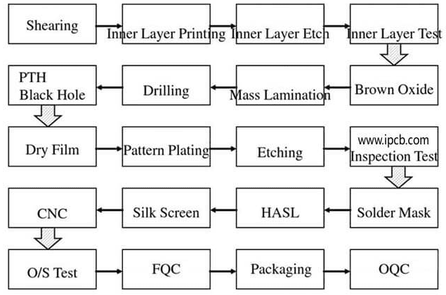
- Material Cutting: The raw copper-clad laminate is cut into panels suitable for the production line, typically around 40*50cm.
- Via Drilling: CNC drills create through-holes connecting the top and bottom layers.
- Through-Hole Plating (PTH): After drilling, the non-conductive hole walls are plated with a thin layer of copper using a chemical deposition process.
- Panel Plating: The initial copper layer from PTH is insufficient. Electroplating is used to increase copper thickness to meet standards (e.g., 20-26µm).
- Dry Film Lamination: A photosensitive dry film is applied to the panel. This film acts as a pattern carrier for the circuit formation.
- Circuit Exposure: A circuit film (photomask) is aligned with the panel. The dry film is exposed to UV light through the mask, hardening the areas not protected by the circuit pattern.
- Circuit Etching: The unexposed dry film is removed, exposing unwanted copper, which is then etched away using chemicals like sulfuric acid, leaving the desired circuit pattern.
- Solder Mask Application: A solder mask ink is applied via screen printing or coating to protect the copper traces and prevent solder shorts during assembly. Common colors are green, blue, red, white, and black.
- Silkscreen Printing: Text, component designators, and logos are printed onto the board, typically in white or black.
- Surface Finish: The exposed copper pads are coated with a surface treatment (e.g., HASL, ENIG) to prevent oxidation and ensure good solderability.
- Panel Profiling/Routing: The assembled panel is cut into individual boards (singulation) using CNC routing or punching, creating the final shape, V-cuts, bevels, slots, etc.
- Electrical Testing: Boards are tested for opens or shorts using flying probe or fixture-based testers. Impedance and high-voltage tests may also be performed.
- Final Quality Control (FQC): Boards undergo visual inspection for appearance, dimensions, hole sizes, thickness, and markings to ensure they meet customer requirements. Qualified boards are then vacuum-packed for shipment.
What Components Are on a PCB?
Below is a list of common PCB components used in manufacturing:
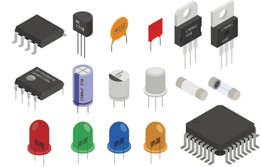
- Capacitors
Capacitors store electrical charge within the circuit and release it when extra power is needed elsewhere. They typically consist of two conductive plates separated by an insulating layer. - Inductors
Similar to capacitors, inductors store energy but are primarily used to suppress signals within the PCB, blocking interference from other electrical devices. - Resistors
Resistors transmit current to create a voltage drop and release electrical energy as heat. They are made from various materials, and the type used depends on the product’s requirements. - Sensors
These devices detect changes in their environment and generate corresponding electrical signals. Other components on the board then use this signal to perform functions. - Transistors
Transistors regulate and control the flow of electrical signals on the PCB. They come in various forms, with bipolar junction transistors being common. - Transformers
Transformers are used to change voltage levels, enabling efficient power transmission across different parts of the PCB’s circuits. - Diodes
Diodes allow current to flow in only one direction, protecting the board and devices from damage due to reverse current flow. Light-Emitting Diodes are a widely used type.
Summary
The PCB is the green board with copper traces and pads, serving as the carrier and connecting backbone for all electronic components. It is the cornerstone of modern electronics. Through precise materials science and sophisticated manufacturing processes, it efficiently and reliably integrates various electronic components, forming the heart and brain of all electronic devices.


0 Comments