




A single-sided PCB has one patterned copper circuit layer, but that does not tell you what supports the copper. Single-sided PCB materials can include paper-based laminates, glass-reinforced composites, glass-epoxy laminates and insulated metal-base constructions. The right choice depends on how the board will be assembled, used and verified, not simply on whether its circuit fits on one side.
For a buyer, the useful question is: which exact construction has been approved for this product? A quotation saying only “single layer, green, 1.6 mm” leaves the material, copper requirement and acceptance evidence unresolved. This guide shows how to close those gaps without confusing a material family with a finished-board guarantee.
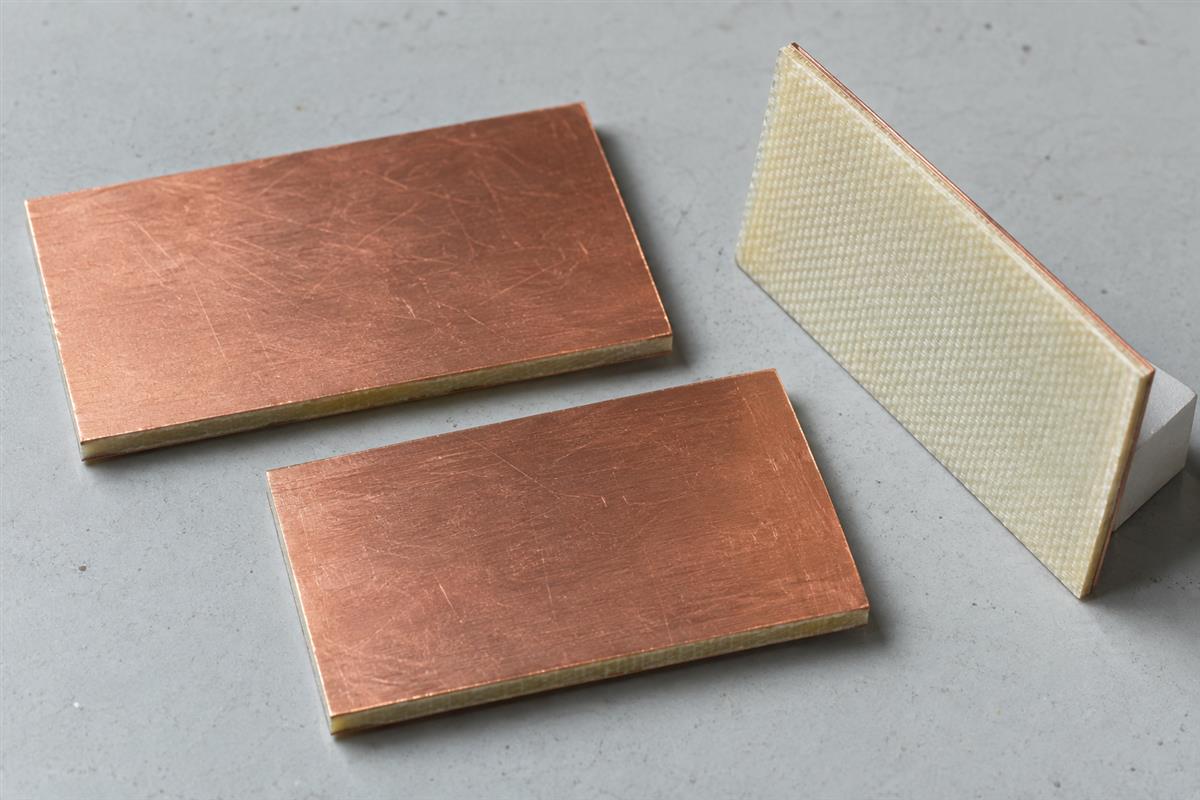
What Is Inside a Single-Sided PCB?
The copper makes the electrical connections; the base material supports and insulates them. “Single-sided” counts the circuit copper layers, not every physical material in the board.
Picture an unassembled board viewed from its copper side. Tracks connect component pads. Between the tracks, the copper has been removed, leaving insulating material beneath. A solder mask may cover the tracks while leaving soldering areas open. Exposed pads may receive a surface finish. Neither solder mask nor pad finish creates a second routing layer.
- Circuit copper: carries current between pads. Its thickness and track geometry must suit the electrical requirement.
- Base material: provides the supporting structure and insulation. Its composition is not determined by copper layer count.
- Solder mask and markings: provide coverage and identification where specified. Their color is not proof of the underlying laminate.
- Pad finish: protects solderable areas under an agreed assembly and storage plan; it is not the substrate.
Component placement is a separate question. Through-hole leads can pass through the base and be soldered to the copper pads, while surface-mount parts can sit directly on copper-side pads. Do not specify a material by assuming that every single-sided board has all components on its non-copper face.
For routing constraints, jumpers and the decision to add another copper layer, see our single-layer PCB routing and selection guide. Here, the focus is the physical construction you purchase and approve.
Compare Materials by Construction, Not Board Color
Compare the material family first, then the actual manufacturer and grade. A brown, pale or green board is not enough evidence to identify its reinforcement, resin system or approved processing limits.
| Candidate | What supports the circuit | Question to settle before choosing it |
|---|---|---|
| FR-1 paper-phenolic | Paper reinforcement with phenolic resin | Does the named grade suit the intended soldering process, environment and mechanical loading? |
| CEM-1 composite | Paper-core and glass-cloth composite with an epoxy-based resin system | Are hole formation, soldering and any proposed hole metallization compatible with this grade? |
| FR-4 glass-epoxy | Glass-reinforced epoxy laminate | Which grade and documented properties are required, rather than merely “FR-4”? |
| Insulated metal substrate | Circuit copper separated from a metal base by an insulating dielectric | How will heat reach the housing or heat sink while electrical isolation is maintained? |
A concrete example is Sunhayato’s No.13 copper-clad board, specified as single-sided FR-1 paper-phenolic with a 1.6 mm board thickness and 35 micrometer copper. That is one product specification, not a rule that every single-sided board uses those dimensions or that FR-1 is interchangeable with another laminate.
Kingboard’s composite-laminate family includes glass-and-paper constructions. Its separate FR-4 range lists multiple grades with different properties. These are useful reminders that a family name is the beginning of selection, not the end.
For metal-base boards, Henkel’s Thermal Clad guide describes a copper circuit, insulating dielectric and metal base. The metal base is not automatically a second patterned circuit layer. Nor does it eliminate the need to design the board-to-heat-sink interface. Ask for the actual construction rather than treating “aluminum PCB” as a complete thermal specification.
Flexible single-sided circuits are another construction category. If bending is part of the job, state the bend requirement and request a suitable flex construction instead of choosing from a rigid-board comparison alone.
Choose the Material Around Assembly and Service Conditions
Start with the conditions the board must survive, then ask which available grade meets them. Choosing the lowest quoted laminate before defining those conditions makes otherwise reasonable quotations difficult to compare.
- Describe the assembly sequence. State whether the board sees hand soldering, wave/selective soldering, reflow or a combination. Include expected rework. Ask the fabricator and assembler to confirm compatibility with the actual time-temperature profile, not just a label such as “lead-free.”
- Describe the operating environment. Identify enclosure temperature, nearby heat sources, humidity or condensation exposure, and electrical isolation needs. Keep operating requirements separate from short manufacturing heat exposure.
- Describe mechanical demands. Show mounting points, connector insertion loads, unsupported spans and thickness constraints. A board that fits the enclosure can still flex unacceptably when a connector is inserted.
- Confirm the production construction. Obtain the named material, thickness tolerance, copper requirement, hole details and proposed fabrication route. Resolve exceptions before a sample order becomes a production order.
Example: suppose a low-voltage control board has one copper layer, through-hole connectors and a snap-fit enclosure. It is tempting to approve a cheaper substrate because the circuit still works on the bench. But the enclosure fit, connector loading and assembly heat exposure remain separate checks. Test the proposed production construction in the enclosure and through the intended assembly sequence. A successful electrical power-up alone does not settle those questions.
Do not assume a particular material family is always cheapest. Compare quotations at the same quantity and acceptance requirements, including tooling, assembly and qualification work. If a proposed substitution introduces new validation work, that cost belongs in the decision.
Read a Material Data Sheet Without Mixing Up the Ratings
Read each number together with its grade suffix, test method, specimen and exposure condition. An impressive-looking number taken out of that context can lead to the wrong purchase specification.
For example, Kingboard’s KB-5150 family data sheet distinguishes CTI values of 175, 300 and 600 V by grade suffix. CTI concerns tracking resistance under a defined test; it is not permission to operate the finished board at that voltage. The same sheet gives a short thermal-stress test condition of 260 degrees Celsius and cautions against plated-through-hole processing for this family. Neither statement should be generalized to every CEM-1 grade.
| Data-sheet item | Do not conclude | Instead ask |
|---|---|---|
| Short solder/thermal exposure | “The board can operate continuously at this temperature.” | What processing profile is allowed, and what separate service-temperature evidence applies? |
| CTI or a flame classification | “This proves the whole product is electrically safe.” | What product-level insulation, spacing and approval requirements still apply? |
| A typical property value | “Every delivered board is guaranteed to meet exactly this value.” | What limit, test condition and acceptance evidence are contractually agreed? |
| Nominal thickness or copper weight | “This is the exact finished dimension.” | What is the tolerance, and is the figure for the starting laminate or finished board? |
Keep the data-sheet revision with the approved material record. When a supplier proposes “equivalent,” compare the properties relevant to your design and process rather than counting how many rows look similar. For general laminate documentation, our copper-clad laminate specification guide explains the broader purchasing checks.
Verify a Material Change Before Releasing Production
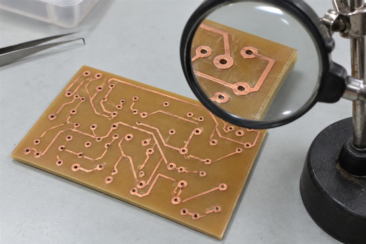
A material change needs approval against the product’s requirements even when the Gerber artwork stays identical. Geometry alone does not verify the new substrate, assembly compatibility or mechanical behavior.
This matters when an early prototype uses one material and production is quoted in another. The prototype may prove the circuit connections while leaving production-material questions unanswered. Treat the change as a controlled engineering decision, not as an invisible purchasing substitution.
- Match the paperwork: manufacturer, grade, revision and construction must agree across the quote, drawing and supplied material evidence.
- Check representative samples: use the proposed production material and the intended fabrication and assembly sequence.
- Inspect the result: look for lifting pads, blistering, cracks, unacceptable distortion or damage around holes. Record findings against agreed acceptance criteria.
- Verify the application: include functional checks, enclosure fit, connector loading and environmental or insulation tests that the product requires. A generic test list cannot replace the responsible engineer’s qualification plan.
- Close the change: identify who approved it, what was tested and which drawing revision now permits the material.
For a hypothetical change from a glass-epoxy prototype to a paper-core production construction, do not simply reuse the prototype approval report. Request production-material samples and assess the differences that matter to the design. If the construction cannot be documented or the required tests have not been agreed, keep the change pending rather than calling it equivalent.
Do not attempt identification by burning, sanding or chemically attacking a populated board. Use drawings, supplier traceability and qualified analysis where necessary. Visual inspection can find damage; it cannot certify the resin system.
Put the Single-Sided Construction in the Purchase Specification
Specify both what must be built and what evidence will demonstrate compliance. The table below is a working checklist to complete with your fabricator, not a universal material recipe.
| Purchase field | What to enter or resolve | Evidence to request |
|---|---|---|
| Circuit construction | One patterned copper layer; identify the copper side and any special base construction | Approved drawing or construction note |
| Material | Manufacturer and grade, or an explicitly controlled approved-material list | Current data sheet and material traceability |
| Dimensions | Finished thickness/tolerance, outline and critical hole requirements | Agreed dimensional inspection results |
| Copper and holes | Starting versus finished copper requirement; plated/non-plated hole distinction | Fabricator’s written construction confirmation |
| Mask and finish | Required coverage and pad finish; assembly/storage constraints | Drawing confirmation and applicable acceptance checks |
| Use and assembly | Thermal exposure, mechanical loading and relevant environment | Agreed compatibility and qualification plan |
| Substitution control | No material change without designated approval | Change record tied to product and drawing revision |
A useful purchase note is: “Supply the material grade and construction shown on the approved drawing. Submit proposed material changes, supporting data and required validation before manufacture.” Complete the drawing first; this wording cannot rescue missing technical requirements.
To discuss a single-sided board with PCBtry, send the Gerber and drill files, fabrication drawing, quantity, proposed material and assembly conditions through the contact page. Identify any unresolved thickness, copper or material-substitution questions and ask for written feasibility confirmation before ordering. Availability and acceptance requirements must be confirmed for the actual job.
Frequently Asked Questions
Does single-sided mean the board is made of FR-4?
No. It describes the circuit copper layer count. The material must be specified separately. Check the approved drawing and material grade rather than assuming that all rigid boards use the same substrate.
Can a single-sided PCB be green?
Yes. Green is commonly a solder-mask color, not a substrate identity. The same visible mask color can conceal different base materials, so a photograph is not sufficient material evidence.
Is CEM-1 interchangeable with FR-4?
Not automatically. They are different constructions. Approve a substitution against the required fabrication, assembly, mechanical and environmental conditions; matching the board outline is insufficient.
Does one copper layer mean there are no holes?
No. Component leads, fasteners and locating features may need holes. State which holes are non-plated and flag any metallization requirement for explicit fabricator review.
Is 1.6 mm a required single-sided PCB thickness?
No. It is a product option, not a definition. Select thickness and tolerance for the design and confirm availability. Nominal thickness alone does not establish enclosure fit.
Does an aluminum base count as another routing layer?
Not by itself. In a one-circuit-layer insulated metal substrate, the base is separated from the copper by dielectric. Obtain the construction drawing to establish its electrical role and any intentional connection.
Can a functional test prove the correct material was supplied?
No. A functional test checks behavior under its test conditions. Material identity requires documentation and traceability, with further verification if the specification calls for it.
What should I do if a supplier lists only “equivalent material”?
Request the proposed manufacturer, grade, data sheet and differences from the approved construction. Agree the necessary validation and record approval before production; do not infer equivalence from a lower price.



0 Comments