
Introduction
Printed Circuit Board (PCB) design has evolved into a distinct specialty within the electronics industry. PCBs play a vital role by providing electrical interconnections between components, rigid support for mounting those components, and a compact package that can be integrated into the final product. They are the primary components in electronic devices that determine their form and function, enabling advanced semiconductors to communicate with each other at extremely high data rates. What are the PCBs on PCB board?
What is a Printed Circuit Board?
A Printed Circuit Board (PCB) is an electronic assembly that uses copper conductors to create electrical connections between components. The PCB also provides mechanical support for electronic components, allowing the device to be housed within an enclosure.
All PCBs are constructed from alternating layers of conductive copper and electrically insulating material. The conductive features on a PCB include copper traces, pads, and conductive planes. The mechanical structure is composed of insulating material laminated between the conductor layers. The overall structure is plated and covered with a non-conductive solder mask, upon which a silkscreen legend is printed to indicate component placement. After these manufacturing steps are completed, the bare board is sent to a PCB assembly house where components are soldered onto it, and the resulting PCBA is tested.
Types of PCBs
1. Single-Sided PCB
The single-sided PCB is the simplest of all manufacturable PCB types. It consists of a single layer of traces (typically copper) located on only one side of the board. Components are mounted on one side, while the interconnected conductive traces are on the other.
- Characteristics:
- Components are placed on only one side.
- Production costs are generally low due to fewer steps involved in design and manufacturing.
- Advantages:
- Cost-effective and relatively simple to manufacture.
- Disadvantages:
- Only suitable for low-density and simple circuits, making it unsuitable for complex designs.
- Applications:
- Calculators and small remote controls.
- Power supplies.
- Small appliances and basic sensor technology.
- For most electronics learners, single-sided PCBs are entry-level boards, ideal for learning PCB layout and implementation due to their simple design.
2. Double-Sided PCB
Unlike single-layer PCBs, double-sided PCBs have copper layers on both the top and bottom layers. Hardware components can be placed on both sides of the board, and connections between the two sides are made through plated through-holes that pass through the board. Double-sided PCBs are among the most widely used PCB types.
- Characteristics:
- Two layers of conductive material with the same dimensions and shape are used in the circuit to conduct current.
- Components can be placed on both sides of the PCB.
- Holes or vias connect the top and bottom layers of such circuits.
- Advantages:
- Higher circuit density within the same area compared to single-sided PCBs.
- Greater design flexibility.
- Capable of handling more complex designs than single-layer PCBs.
- Applications:
- Industrial controls.
- Power monitoring systems.
- LED lighting.
- Double-sided PCBs are slightly more complex than single-sided types and more capable of handling intricate designs, yet easier to produce than multilayer PCBs.
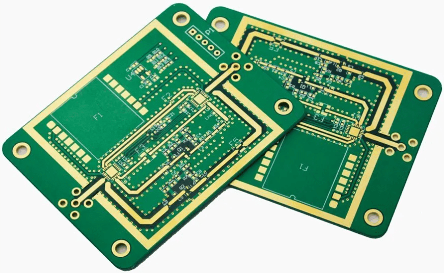
3. Multilayer PCB
Multilayer PCBs elevate complexity to a new level, featuring thin layers of conductive material stacked together with insulating material sandwiched between them, resulting in three or more layers. Interconnections between layers are achieved through vias. Consequently, circuits can be designed to be more complex with finer pitch. Multilayer PCBs are among the more advanced PCB types.
- Characteristics:
- Can have many layers, commonly 4, 6, 8, or even more.
- Combines two or more layers of material in a laminated structure with insulation between them.
- The design and manufacturing aspects require more complex processes than other types.
- Advantages:
- High circuit density.
- More compact, resulting in space-saving designs.
- Suitable for most circuits requiring high-speed operation.
- Applications:
- Computers, laptops, and mobile phones.
- Advanced medical equipment.
- Military and aerospace electronics.
4. Rigid PCB
Rigid PCBs are manufactured using a rigid or hard substrate material. They are sturdy and not easily deformed, making them ideal for applications where the board needs to remain rigid and fixed in one position. Compared to flexible PCBs, rigid PCBs are more common among the different types of printed circuit boards.
- Characteristics:
- This printed circuit board is made from rigid materials like FR4 for optimal performance.
- It is solid and non-flexible.
- Often includes one or more layers for data storage/power planes.
- Advantages:
- Durable and reliable.
- Proven to be highly effective for handling complex and dense circuits.
- Suitable for applications mounted in fixed positions.
- Applications:
- Desktop and laptop computer motherboards.
- Hard drives.
- Telecommunication equipment.
- Rigid PCBs form the core physical entity of most traditional electronic devices, providing a solid foundation for the orderly synthesis of all necessary electrical hardware.
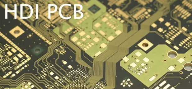
5. HDI PCB
HDI stands for High-Density Interconnect. These PCBs are distinguished by their higher wiring density per unit volume compared to other PCB types. They feature finer trace widths and spacing, smaller via sizes, and higher connection pad densities. HDI PCBs are among the most challenging printed circuit boards to manufacture.
- Characteristics:
- High wiring/routing density.
- Utilizes microvias and blind/buried vias.
- Compact structure and higher integration level due to spatial constraints.
- Advantages:
- Offers optimized performance and reliability.
- Can accommodate more components within the same volume.
- Highly suitable for small devices and compact electronics.
- Applications:
- Smartphones and tablets.
- Wearable technology.
- Advanced computing systems.
- HDI PCBs are widely used in today’s electronics market where PCB performance and compactness are key requirements.
6. Flexible PCB
Another PCB type is the flexible circuit, which uses flexible materials like polyimide. They can bend and flex in various ways to fit into different shapes, making them ideal for compact designs. Flexible PCBs are a special type of printed circuit board.
- Characteristics:
- Uses flexible materials for fabrication.
- Can be bent, twisted, and folded into position.
- Can be single-layer, double-layer, or multilayer depending on needs.
- Advantages:
- Highly flexible and lightweight.
- Compact and can be cleverly integrated into complex geometries.
- Ideal for applications where the PCB might need to flex, as its design allows for this bending.
- Applications:
- Wearable electronics.
- Flexible solar cells.
- Medical devices (e.g., pacemakers, hearing aids).
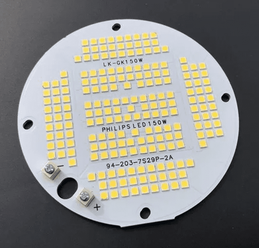
7. Metal-Clad PCB (Aluminum-backed PCB)
Metal Core PCBs (MCPCBs) or Aluminum PCBs utilize a metal backing to enhance thermal conductivity. These PCBs are primarily suitable for applications where heat dissipation is critical.
- Characteristics:
- The common feature of this PCB type is superior thermal dissipation performance.
- Can be single-sided or double-sided, depending on complexity.
- Advantages:
- Efficient thermal management.
- Ideal for high-power applications, offering better energy efficiency compared to standard FR4 PCBs.
- Applications:
- LED lighting.
- Power supplies.
- Automotive electronics.
- Aluminum-backed PCBs are the printed circuit board type used for high-power and high-thermal applications like LED lighting and automotive systems, where heat dissipation is paramount.
8. High-Frequency PCB
High-Frequency PCBs are circuit boards used for circuits operating above 1 GHz. They are made from materials with stable dielectric constants and low signal loss, which is crucial for high-speed, high-frequency operation. High-Frequency PCBs are a specialized type used in microwave and RF applications.
- Characteristics:
- Uses materials like PTFE (Teflon) or RF-specialized laminates.
- Designed for a specific operational frequency range.
- Advantages:
- Excellent signal integrity at high frequencies.
- Low electromagnetic interference (EMI).
- Suitable for transmitting high-speed data.
- Applications:
- Wireless communication systems operating at RF and microwave frequencies.
- Satellite communications.
- High-speed digital circuits.
- Radar systems.
- High-Frequency PCBs are indispensable in markets like telecommunications and satellite communications that require fast and accurate data transmission.
The manufacturing and assembly processes for these PCB types vary. However, with the correct PCB design rules implemented in software, today’s ECAD software can help designers create any of these boards.
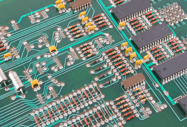
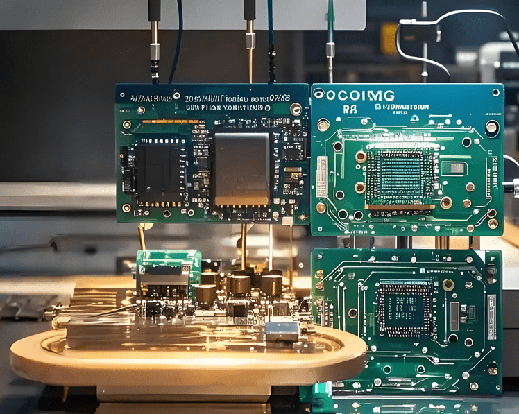
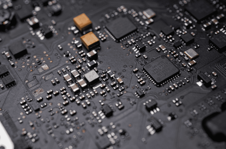
In the image above, we see a vintage circuit board primarily using through-hole components to achieve the desired functionality. Modern printed circuit boards have shifted heavily towards using Surface Mount Device (SMD) components, as they are more practical in high-density, double-sided designs. SMD components are now standard for most applications requiring small size, low power, and low cost. However, some applications still use through-hole components due to their higher reliability and ease of assembly, including manual assembly. The image below shows an example of a modern PCB utilizing high-density SMD components.
PCB Material Composition
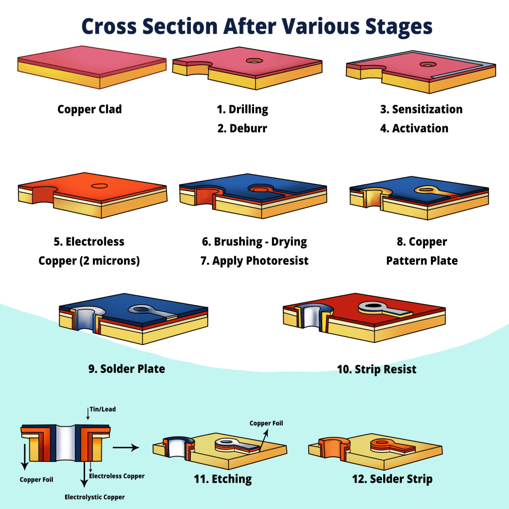
PCBs are typically made from layers that are fused together under heat and pressure to form a single entity. The different types of PCB materials used in a PCB, from top to bottom, include the Silkscreen, Solder Mask, Copper, and Substrate layers.
The bottom layer is the Substrate, made from fiberglass, also known as FR4, where the letters ‘FR’ stand for “Flame Retardant.” This substrate layer provides a solid foundation for the PCB, though its thickness can vary depending on the board’s purpose.
There are also cheaper boards available that use phenolic resin or epoxy instead of the aforementioned PCB substrate materials. These boards are thermally sensitive and can easily delaminate. They are often identifiable by the distinctive smell they emit during soldering.
The second layer is the Copper layer, laminated onto the substrate using a combination of heat and adhesive. The copper layer is thin. Some boards have two copper layers, one on top and one below the substrate. PCBs with a single copper layer are often used in lower-cost electronics.
The widely used Copper Clad Laminate (CCL) can be classified into different categories based on various criteria such as reinforcing material, resin adhesive used, flammability, and CCL performance. A brief classification of CCL is shown in the table below:
| Classification Standard | Material Category | Examples |
|---|---|---|
| Reinforcing Material | Paper-Based | PF Resin (XPC, FR1, FR2), Epoxy Resin (FE-3), Polyester Resin |
| Glass Fiber Fabric-Based | Epoxy Resin (FR4, FR5) | |
| Composite Epoxy Material (CEM) | / | |
| Laminated Multilayer Base | / | |
| Special Material Base | BT, PI, PPO, MS | |
| Flammability | Flame Retardant | UL94-V0, UL94-V1 |
| Non-Flame Retardant | UL94-HB | |
| CCL Performance | Standard Performance CCL | / |
| Low Dielectric Constant CCL | / | |
| High Heat Resistance CCL | / | |
| Low Coefficient of Thermal Expansion CCL | / |
Above the green Solder Mask layer is the Silkscreen layer, used to add letters and number indicators. This allows technicians and assemblers to easily read identifiers on the PCB, making it simpler to place each component in the correct location and orientation. The silkscreen layer is typically white, but other colors like red, yellow, gray, and black are also sometimes used.
PCB Layer Technical Terminology
Beyond understanding how PCBs are layered, you should also be familiar with the technical terminology associated with PCB usage:
- Annular Ring. The ring of copper surrounding a hole on a PCB.
- DRC. An abbreviation for Design Rule Check. Essentially, DRC is a method for checking the functionality of a PCB design. Details checked include trace width and drill hole sizes.
- Drill Hit. A term describing all holes on a PCB, correct or incorrect. In some cases, due to the use of blunt drill equipment during production, holes may be slightly misaligned.
- Gold Finger. Exposed metal along the edge of a board, used as a connection point between two PCBs. Gold fingers are most commonly found on older video game cartridges and memory cards.
- Mouse Bite. A portion of the PCB that is over-drilled to the point where it threatens the board’s structural integrity.
- Pad. An exposed metal area on the PCB, typically where solder is applied to attach a component.
- Panel. A large board composed of smaller boards, which are eventually separated for individual use.
- Solder Paste Stencil. A metal stencil placed over the board to apply solder paste to specific areas for soldering.
- Plane. A large area of exposed copper on the PCB, defined by a border but containing no traces. Used for power and ground.
- Plated Through-Hole. A hole drilled directly through a PCB, typically used to connect another component. The hole is plated and usually has an annular ring.
- Slot. Any hole that is not circular. PCBs with slots typically cost more because producing non-circular holes is more expensive. Slots are often non-plated.
- Surface Mount. A method of mounting external parts directly onto the PCB without using through-holes.
- Trace. A continuous path of copper running across the PCB.
- V-Score. A partial cut through the board, making the PCB easy to break along a line.
- Via. A hole used for a signal to pass from one layer to another. A tented via is covered with protective solder mask, while an untented via might be used for connector access.
The number preceding the layer count refers to the specific number of conductive layers, whether they are routing layers or plane layers. The layer count is typically 1, or the next even numbers: 2, 4, 6, 8. Boards with odd layer counts are rare and generally offer little practical benefit. For instance, the PCB substrate for a 5-layer board is almost identical to that of a 6-layer board.

These two layer types serve different functions. Routing Layers contain tracks (traces). Plane Layers act as power connectors (e.g., VCC, GND) and feature large copper planes. Plane layers can also have isolated copper areas (islands) defined for specific signal voltages, such as 3.3V or 5V.
FR4 is the designation for Glass Reinforced Epoxy Laminate Sheet. Due to its high strength, moisture resistance, and good flame-retardant properties, FR4 is one of the most popular materials among all PCB material types.
Starting a New PCB Design
When starting a new design, a printed circuit board goes through several stages. Production-grade board designs use ECAD software, or CAD applications containing numerous utilities dedicated to board design and layout. ECAD software is built to help designers through the specific workflow of board design, starting with drawing basic electrical schematics and ending with preparing files for manufacturing. The board design follows this basic workflow:
- Front-End Engineering – At this stage, major components are selected, and basic circuit diagrams are often created to define the board’s functionality.
- Schematic Capture – In this stage, simple circuit diagrams are converted into electronic drawings defining electrical connections between components using ECAD software. Schematic symbols are used to represent components in the design.
- Material Selection and PCB Stack-up Design – Here, laminate materials are selected, and the layer stack-up is designed to meet requirements for plane layers, signal layers, dedicated routing channels, and specific material properties.
- Component Placement – After setting the board shape and importing components into a new PCB layout, components are arranged within the layout to meet the design’s mechanical requirements.
- Routing – Once the component layout is approved, routing (track placement) between components can begin. Routing tools in the ECAD software are used to set trace geometry. During this phase, trace geometry can be determined to ensure impedance control (for high-speed signals).
- Design Review and Verification – After routing is complete, it’s best practice to inspect and evaluate the design to ensure there are no errors or unresolved issues. This can be done through manual checks or by using post-layout simulation tools.
- Manufacturing Preparation – Once the design is finalized, standard manufacturing files are generated to prepare for production. These files are used to automate manufacturing and assembly equipment.
If you want to move through all these stages of the PCB electronic board design process easily, you need to use the best design software with an intuitive user interface and a complete set of PCB design features.
Creating Printed Circuit Boards with Altium
The industry’s best ECAD software should be easy to use, easy to learn, and include a complete, unified set of design features. Altium integrates everything into a single platform, allowing you to complete your design and prepare it for production without needing any external programs.
- Altium provides you with everything needed to turn your ideas into reality. You can build a wide range of products, from simple single-sided boards to advanced high-density electronics.
- Altium’s user interface is built upon an integrated design rules engine, ensuring all your design functions work together within a single program.
- Design teams use Altium to stay efficient and share design data in a secure cloud environment.
Altium’s integrated design environment provides everything needed to design and manufacture high-quality printed circuit board assemblies. Other programs fragment your critical design tools across different programs with disparate workflows, making it difficult to stay efficient and increasing licensing costs. Altium is consistently rated the easiest-to-learn and easiest-to-use design environment, making it ideal for both new and experienced design professionals.
Summary: Two Interdependent Disciplines
- The PCB is the physical entity, the final physical carrier of electronic function.
- PCB Design is the process, the creative intellectual activity that gives the PCB its life and soul.
Without excellent PCB design, even the best circuit方案 cannot achieve stable, efficient, and reliable functionality. Conversely, without the PCB as a carrier, the design is merely a castle in the air. It is the perfect combination of PCB design and PCB manufacturing that forms the cornerstone of the modern electronics industry, driving our digital world forward.
It can be said that behind every intricate circuit board lies the wisdom and effort of PCB designers, who use invisible lines to weave the visible intelligent world we inhabit.


0 Comments