
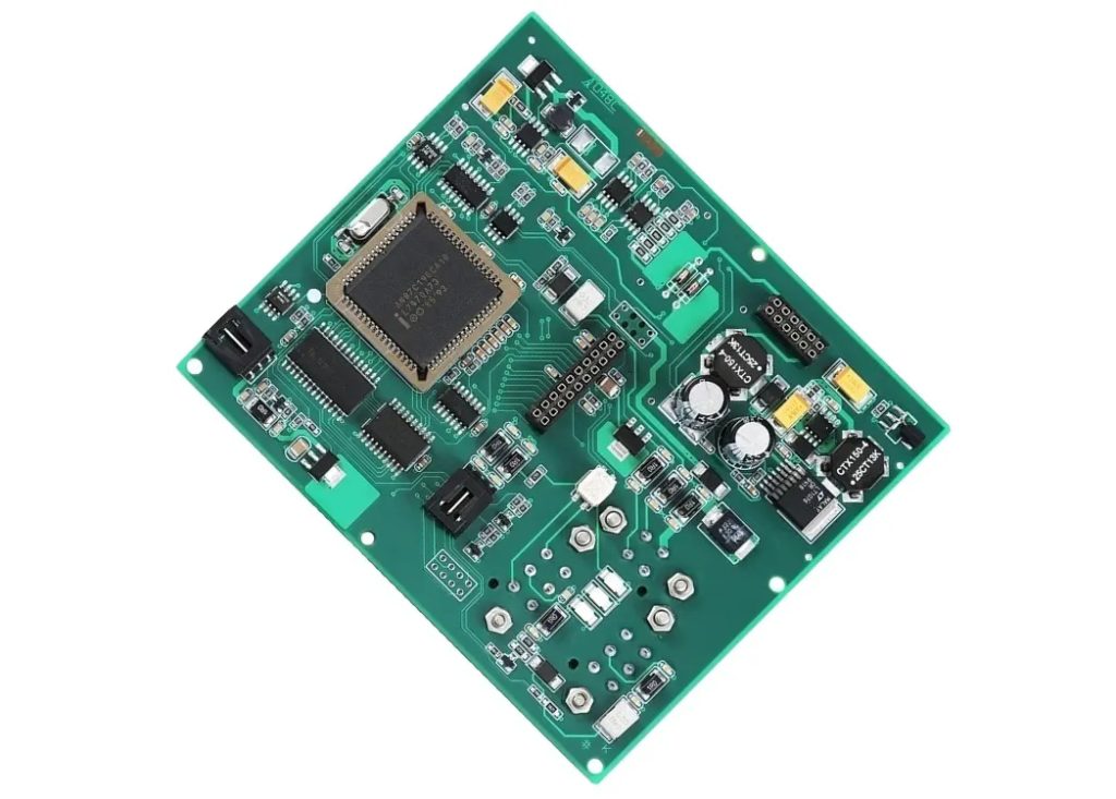
In the rapidly evolving electronics industry, a bare PCB board(Printed Circuit Board) refers to a manufactured circuit board that includes copper traces and vias, primarily serving as the structural foundation for electronic connections. Essentially, it’s a PCB without any components mounted. While a bare PCB board itself doesn’t have any functional purpose, it is crucial in the entire PCB manufacturing process, as most testing and manufacturing processes are performed on the bare board.Understanding its types, manufacturing processes, pricing, and applications is essential for engineers, manufacturers, and businesses. This guide will provide a comprehensive overview of bare PCB board and explain how to ensure quality and performance through professional manufacturing services.
What is a bare PCB?
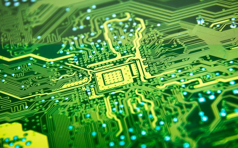
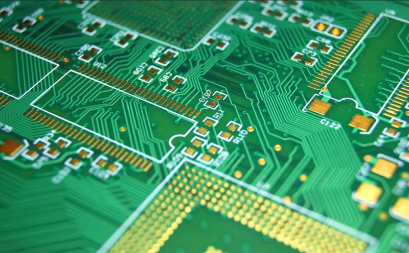
A bare PCB board is a printed circuit board that has no electronic components soldered to it. It consists of conductive traces, solder pads, and layered structures, designed to facilitate signal transmission and power distribution between electronic components after assembly. However, the bare PCB board itself cannot function; it only becomes functional after components are mounted, allowing for testing and achieving its intended purpose. Essentially, a bare PCB board can be considered the “skeleton” of any electronic device.
What are the main components of a bare PCB board?
Substrate Material: The substrate is the supporting framework of the PCB, providing insulation and structural support. Common materials include FR-4 fiberglass-reinforced epoxy resin, ceramic, and polyimide (PI). Different materials are suitable for various applications, such as consumer electronics, high-frequency communications, and automotive electronics.
Copper Layer: The copper layer is the conductive part of the PCB, used for wiring and signal transmission. A single-layer PCB has only one layer of copper foil, while multilayer boards achieve complex circuit designs through multiple copper layers.
Solder Mask: The solder mask is usually green (but can be other colors), covering the copper layer to prevent short circuits during soldering and protect the circuit from oxidation and contamination.
Silk Screen Layer: The silk screen layer is typically white and used to mark text, symbols, and component locations on the circuit board, facilitating assembly, testing, and maintenance.
Surface Finish Layer: The surface finish layer covers the solder pads and any exposed copper areas not covered by the solder mask, providing protection. Common surface finish methods include HAL, ENIG, OSP, immersion silver, immersion tin, and ENEPIG.
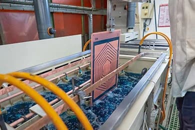
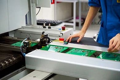
Bare PCB Manufacturing Process
The manufacturing process of a bare PCB board is a systematic and meticulous process involving multiple steps. It typically includes the following key steps:
Design and Layout: Using EDA tools, create the circuit diagram and generate the PCB layout, defining traces, vias, and pads as the basis for production.
Photomasking and Image Transfer: After DFM (Design for Manufacturing) review of the design files, transfer the circuit pattern onto the copper foil substrate using a photomask, followed by photolithography and etching to form the desired circuit pattern.
Excess Copper Removal and Inspection: Remove unwanted copper layers, leaving only the designed circuit area, and perform visual and data comparison inspections to ensure accuracy.
Lamination and Drilling: Laminate the multi-layer board and drill holes at specified locations to prepare for subsequent electrical connections.
Plating and Final Etching: Deposit a copper layer and tin plating on the holes and surface, and then etch again to form complete traces and pads.
Solder Mask and Surface Treatment: Apply a solder mask for circuit protection, and perform surface treatment (e.g., ENIG, OSP) according to process requirements to enhance solderability and durability.
Silk Screening and Electrical Testing: After printing markings (text, symbols, etc.), perform electrical performance tests on the circuit board to ensure no short circuits or open circuits.
Panelization and Separation
Separate individual PCBs from the panel using a cutting process. This process ensures that the bare PCB board has good electrical performance and mechanical stability before entering the assembly stage, thus completing the bare PCB board manufacturing process.
Differences between Bare PCB and Zero PC Boards
Although their names are similar, bare PCB board and Zero PC boards (universal PCB boards) have distinct differences in definition and usage:
Bare PCB Board
This refers to a circuit board manufactured according to a specific circuit design, but without any electronic components soldered on. It is customized and typically used in the mass production of electronic products, providing the foundation for subsequent component assembly.
Zero PC Board
Also known as a universal PCB board, this is a non-customized circuit board. Its solder pads are usually arranged in a grid pattern, without any solder mask or silkscreen layer; all pads can be used to connect different components. Due to its flexible structure, it functions similarly to a breadboard and is commonly used for prototyping, testing, and evaluating small circuits or circuit modules.
In short, a bare PCB board is the basic circuit board for mass-produced products, while a Zero PC board is more like a tool for experimentation and development, with completely different functionalities and application scenarios.
Types of Bare PCB Board
Bare PCB board can be categorized into several types depending on their application:
Single-sided PCB: The circuitry is located on a single side of the board, making the manufacturing process simpler.
Double-sided PCB: Circuit layers are present on both sides of the board, offering wider application possibilities.
Multi-layer PCB: Multiple layers are stacked together, suitable for high-density designs.
High-temperature resistant PCB: This type of PCB maintains stable performance even under high temperatures, and is primarily used in electronic devices that require long-term operation under high power, high temperature, or high thermal shock conditions.
Electrical Testing of Bare PCB Board
Before bare PCB board can be used, they must undergo rigorous electrical testing to ensure their performance and reliability.
Common electrical test items include:
Resistance Test: Measures the resistance between different nodes to verify that the electrical performance meets design requirements.
Insulation Test (also known as Insulation Resistance Test): Verifies that the insulation between different nodes is sufficient to prevent short circuits.
Capacitance Test: Measures the capacitance between nodes to ensure the circuit meets design specifications.
Connectivity Test: Checks the conductivity of each node within the same network structure to confirm that there are no open circuits.
Flying Probe Test: A widely used and efficient testing method, the flying probe test can quickly perform connectivity and short-circuit checks, as well as various other tests such as resistance, capacitance, and impedance. Its flexibility, accuracy, and lack of need for specialized test fixtures make it a popular method among PCB manufacturers.
In addition, for high-precision and complex PCB, the following tests may also be required:
Impedance Verification: Ensures that the impedance of specific traces meets requirements.
Only after passing these tests and obtaining a “test passed” certification can the bare PCB board proceed to the subsequent component placement and assembly processes.
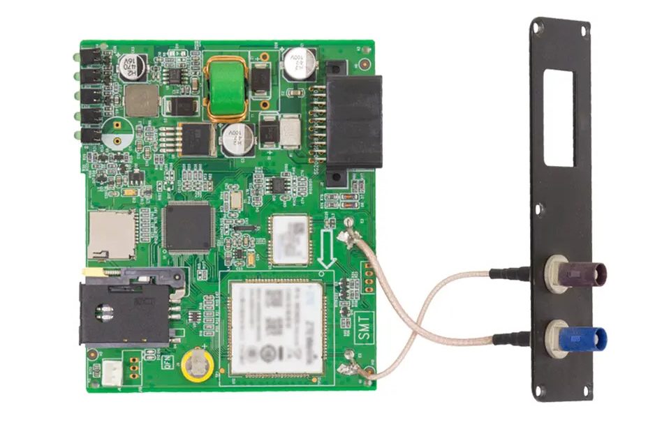
Applications of Bare PCB Board
Bare PCB board are used in almost all electronics industries:
Consumer electronics: Smartphones, tablets, wearables
Automotive electronics: ADAS systems, electric vehicle battery management
Medical devices: Imaging systems, portable diagnostic equipment
Communication equipment: 5G base stations, networking equipment
Industrial automation: Robotics, smart factories
Different industries have varying performance requirements for PCBs; professional manufacturing ensures their stability and reliability.
Reliable PCB Manufacturing and Prototyping Services
Thindry’s bare PCB product line offers you a smooth and efficient development experience:
Professional Design Review
Our team of experienced engineers reviews your design files to ensure the production feasibility of your bare PCB and helps you avoid potential board-level issues.
High-Quality Production
We collaborate with numerous reliable suppliers to produce your bare PCBs to the highest quality standards.
Advanced Manufacturing Processes
To meet your design needs, we offer a variety of advanced PCB manufacturing technologies, such as plated through-holes, impedance control, blind vias, buried vias, and microvia technology.
One-Stop Assembly Service
With advanced equipment and years of industry experience, Thindry is committed to providing customers with high-quality, high-efficiency PCB solutions, helping businesses accelerate innovation.


0 Comments