
A multilayer PCB is used when a circuit needs more routing space, better signal control, higher component density, or stronger power distribution than a single-sided or double-sided board can provide. In real projects, multilayer boards are common in automotive electronics, industrial control, medical devices, communication equipment, servers, AI hardware, consumer electronics, and power systems.
For engineers and purchasing teams, the challenge is not only choosing the right layer count. A reliable multilayer PCB also depends on stack-up design, material selection, impedance control, lamination quality, via structure, copper thickness, thermal performance, testing, and supplier capability. This guide explains the key points in a practical way, based on how multilayer PCBs are actually designed, reviewed, manufactured, inspected, and purchased.
Thindry is a China-based PCB manufacturer and assembly service provider founded in 2005. With experience in PCB prototype, fabrication, component sourcing, and PCBA assembly, Thindry supports customers from design validation to volume production through a digitalized one-stop electronics manufacturing workflow.
What Is a Multilayer PCB?
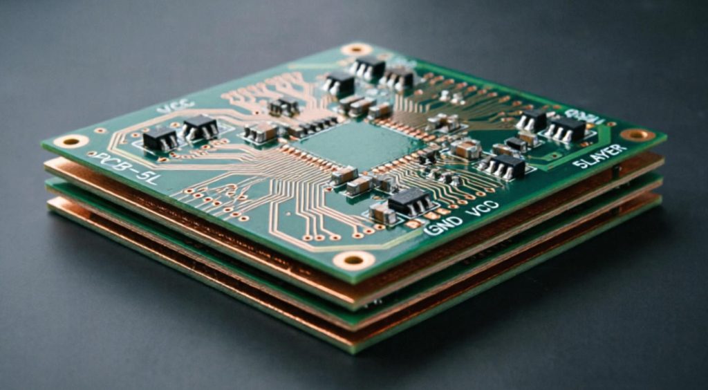
A multilayer PCB is a printed circuit board made with three or more conductive copper layers, separated by insulating dielectric materials. These layers are laminated together under heat and pressure to form one solid board. In most commercial and industrial applications, common multilayer PCB structures include 4-layer, 6-layer, 8-layer, 10-layer, 12-layer, and higher layer-count designs.
Compared with a double-sided PCB, a multilayer printed circuit board gives engineers more freedom to route complex circuits. It can include dedicated signal layers, power planes, and ground planes. This improves routing density, helps reduce electromagnetic interference, and supports controlled impedance for high-speed or RF signals.
In simple terms, a multilayer PCB allows more circuit functions to fit into a smaller and more stable structure. That is why it is widely used in compact, high-speed, high-reliability electronics.
Why Multilayer PCB Design Matters
Multilayer PCB design matters because every layer affects electrical performance, manufacturability, cost, and long-term reliability. A board may look correct in layout software but still be difficult to manufacture if the stack-up is unbalanced, the dielectric thickness is unsuitable, the via design is risky, or the copper distribution is poor.
Good multilayer PCB design helps control signal return paths, reduce noise, improve power integrity, manage heat, and make production more stable. Poor design can lead to impedance mismatch, delamination, warpage, via cracking, assembly defects, or unstable field performance.
- It supports higher routing density in compact products.
- It improves high-speed signal performance when stack-up is designed correctly.
- It reduces electromagnetic interference through proper ground and power planes.
- It helps separate analog, digital, RF, and power circuits.
- It improves production repeatability when design rules match factory capabilities.
How a Multilayer PCB Works
A multilayer PCB works by using several copper layers to carry signals, power, and ground connections inside one laminated board. Outer layers usually carry components and surface routing, while inner layers may be used for signal routing, power distribution, or ground reference planes.
Vias connect different layers together. A standard through-hole via passes through the entire board. Blind vias connect an outer layer to one or more inner layers without going through the full board. Buried vias connect only internal layers. In HDI multilayer PCB designs, microvias are often used to save space and improve routing density.
The stack-up is the foundation of the board. It defines the order of copper layers, dielectric thickness, core materials, prepreg materials, copper weight, and impedance targets. For high-speed, RF, automotive, or medical applications, stack-up planning should be confirmed early with the PCB manufacturer, not left until the final production stage.
Main Types of Multilayer PCB
Multilayer PCBs are not all the same. The right type depends on the product structure, signal speed, current load, temperature environment, bending requirement, and reliability target.
| Type | Typical Use | Main Advantage | Common Challenge |
|---|---|---|---|
| Standard Rigid Multilayer PCB | Industrial controls, consumer electronics, instruments | Stable structure and mature manufacturing process | Requires careful stack-up and drilling control |
| HDI Multilayer PCB | Smart devices, wearables, cameras, compact modules | High routing density and smaller board size | Higher process complexity and cost |
| High-Speed Multilayer PCB | Servers, AI hardware, switches, communication systems | Better impedance and signal integrity control | Material selection and insertion loss become critical |
| High-Frequency Multilayer PCB | RF modules, antennas, radar, satellite communication | Low dielectric loss and stable RF performance | Requires specialized materials and tight process control |
| Heavy Copper Multilayer PCB | Power electronics, chargers, battery systems, inverters | Handles higher current and improves thermal capacity | Etching, lamination, and copper balance are more difficult |
| Rigid-Flex Multilayer PCB | Medical devices, cameras, aerospace electronics, wearables | Combines rigid assembly areas with flexible interconnects | Bend radius, material transition, and cost must be controlled |
Common Materials Used in Multilayer PCB Manufacturing
Material choice has a direct impact on electrical performance, thermal behavior, mechanical stability, and cost. Many standard multilayer PCBs use FR-4-based laminates, but advanced projects may require high-Tg, low-loss, metal-backed, flexible, or RF materials.
For general electronics, FR-4 is widely used because it is cost-effective and suitable for many applications. For automotive, industrial, power, and high-temperature environments, high-Tg materials are often preferred. For high-speed and RF applications, low-loss materials help reduce signal attenuation and improve stable transmission.
| Material Category | Common Application | Key Benefit | Selection Note |
|---|---|---|---|
| Standard FR-4 | Consumer, industrial, general electronics | Good balance of cost and performance | Check Tg, CTI, thickness, and copper weight |
| High-Tg FR-4 | Automotive, power, industrial control | Better thermal resistance | Useful for lead-free assembly and high-temperature operation |
| Low-Loss Material | High-speed digital systems | Lower signal loss | Important for high data-rate designs |
| High-Frequency Material | RF, microwave, radar, antenna systems | Stable dielectric performance | Requires careful processing and impedance planning |
| Polyimide | Flexible and rigid-flex PCB | Good flexibility and heat resistance | Bending structure should be reviewed early |
| Metal Core or Thermal Materials | LED, power modules, thermal designs | Improved heat dissipation | Thermal path and insulation requirements must be confirmed |
Multilayer PCB Manufacturing Process
Multilayer PCB manufacturing is more complex than single-sided or double-sided PCB production because the inner layers must be accurately imaged, etched, aligned, laminated, drilled, plated, and inspected. A small error in inner-layer registration or lamination quality can affect the whole board.
- Engineering review: Gerber files, drill files, stack-up, impedance notes, material requirements, and special instructions are checked.
- Inner-layer imaging: Copper patterns are transferred onto inner-layer cores.
- Inner-layer etching: Unwanted copper is removed to form circuit patterns.
- AOI inspection: Inner layers are inspected before lamination because they cannot be repaired easily later.
- Lamination: Cores and prepregs are pressed together under heat and pressure.
- Drilling: Mechanical drilling or laser drilling creates via and through-hole structures.
- Plating: Copper is deposited inside holes to create electrical connections between layers.
- Outer-layer imaging and etching: External copper patterns are created.
- Solder mask and surface finish: Protective coating and pad finish are applied.
- Routing and profiling: The board shape is formed according to mechanical drawings.
- Electrical testing: Open and short circuits are checked.
- Final inspection: Visual, dimensional, and quality inspections are completed before shipment.
For custom multilayer PCB orders, the engineering review stage is extremely important. Many cost and quality problems can be avoided before production if stack-up, drill design, copper thickness, controlled impedance, and panelization are reviewed carefully.
Multilayer PCB Design Rules Engineers Should Not Ignore
Design rules should never be copied blindly from an old project. A 4-layer industrial control board, a 10-layer communication board, and a 20-layer AI server board may all need very different design constraints. The safest approach is to confirm the design rules with the manufacturer before final layout.
- Stack-up planning: Define signal, power, and ground layers early. Do not treat stack-up as a final export detail.
- Impedance control: Confirm target impedance, tolerance, reference layers, dielectric thickness, and copper thickness.
- Via structure: Choose through-hole vias, blind vias, buried vias, or microvias based on routing needs and manufacturing cost.
- Copper balance: Avoid large copper imbalance between layers, as it can increase warpage risk.
- Power integrity: Use suitable power and ground plane design to reduce voltage drop and noise.
- Thermal planning: Add thermal vias, copper areas, and heat paths where components generate significant heat.
- DFM review: Run manufacturability checks before releasing production files.
A practical design rule is simple: do not design to the theoretical limit unless the product really needs it. Using slightly more manufacturable trace width, spacing, via size, and annular ring can often reduce cost and improve yield.
Multilayer PCB Testing and Quality Standards
Testing is one of the most important parts of multilayer PCB production. Because internal layers cannot be visually inspected after lamination, the process must include strict inspection at multiple stages. Reliable manufacturers combine material control, inner-layer AOI, process monitoring, electrical testing, and final inspection.
Common quality references include IPC standards for PCB acceptability and performance, UL requirements for safety-related board recognition, RoHS compliance for restricted substances, and ISO-based quality management systems. For automotive projects, IATF 16949-related manufacturing discipline is often expected. For medical electronics, ISO 13485-related quality control is especially important.
| Test or Standard | Purpose | Why It Matters |
|---|---|---|
| AOI Inspection | Checks copper pattern defects | Detects opens, shorts, nicks, and spacing issues |
| Electrical Test | Checks circuit continuity and isolation | Reduces risk of open and short circuits |
| Impedance Test | Verifies controlled impedance structures | Important for high-speed and RF designs |
| Microsection Analysis | Checks plating, hole wall, layer alignment, and dielectric condition | Useful for process validation and failure analysis |
| Solderability Test | Checks surface finish performance | Helps avoid assembly soldering problems |
| Thermal Stress Test | Evaluates board resistance to thermal cycling or soldering heat | Important for reliability-focused applications |
| RoHS Compliance | Controls restricted hazardous substances | Required for many global electronics markets |
| UL Certified PCB | Supports safety-related material and process recognition | Important for many commercial and industrial products |
Thindry supports PCB production under quality systems and compliance frameworks including ISO 9001, ISO 13485, IATF 16949, UL certified PCBs, and RoHS compliance. These certifications help customers match quality expectations in medical, automotive, industrial, and global electronics markets.
Common Multilayer PCB Failures and How to Prevent Them
Multilayer PCB failures are often caused by a combination of design, material, process, and assembly factors. The root cause is not always obvious from the surface. A board may pass basic visual inspection but fail during thermal cycling, reflow soldering, vibration, high-speed operation, or long-term field use.
| Failure Issue | Possible Cause | Prevention Method |
|---|---|---|
| Delamination | Moisture, poor lamination, unsuitable material, excessive thermal stress | Use qualified laminates, control storage, baking, and lamination parameters |
| Via Cracking | Thermal expansion stress, poor plating, high aspect ratio | Review aspect ratio, plating thickness, material CTE, and thermal cycling requirements |
| Impedance Deviation | Incorrect stack-up, copper thickness variation, dielectric variation | Confirm stack-up before production and use impedance coupons where needed |
| Warpage | Unbalanced copper, uneven stack-up, high temperature stress | Improve copper balance and choose symmetrical stack-up design |
| Soldering Defects | Poor pad design, surface finish issue, oxidation, wrong stencil design | Check land pattern, solder mask opening, surface finish, and assembly process |
| CAF Risk | Conductive anodic filament growth due to moisture, voltage bias, and tight spacing | Use proper material, spacing, cleanliness, and reliability testing |
| Signal Integrity Problems | Poor return path, uncontrolled impedance, bad layer transition | Plan reference planes, via transitions, and high-speed routing rules early |
The best way to prevent failure is to involve the manufacturer early. A short DFM discussion before prototype production can save much more time than troubleshooting after assembly defects appear.
Multilayer PCB vs Double-Sided PCB
Many buyers ask whether they really need a multilayer PCB or whether a double-sided PCB is enough. The answer depends on circuit complexity, board size, signal speed, current requirement, EMI control, and reliability expectations.
| Comparison Point | Double-Sided PCB | Multilayer PCB |
|---|---|---|
| Layer Structure | Two copper layers | Three or more copper layers |
| Routing Density | Limited | Much higher |
| Signal Integrity | Suitable for simple circuits | Better for high-speed and controlled impedance designs |
| EMI Control | More difficult | Improved with dedicated ground and power planes |
| Cost | Lower | Higher due to lamination and process complexity |
| Applications | Simple electronics, LED boards, basic control boards | Automotive, medical, industrial, communication, AI, servers, compact devices |
If the circuit is simple and space is not tight, a double-sided PCB may be the better choice. If the product needs high density, stable reference planes, better EMI control, or high-speed routing, a multilayer PCB is usually the safer option.
Cost Factors in Multilayer PCB Manufacturing
Multilayer PCB cost is affected by much more than board size. Two boards with the same dimensions can have very different prices if one uses standard FR-4 and the other requires high-Tg material, blind vias, tight impedance, heavy copper, or special surface finish.
- Layer count: More layers usually mean higher material, lamination, drilling, inspection, and processing costs.
- Material type: High-Tg, low-loss, RF, flexible, or special materials cost more than standard FR-4.
- Board thickness and copper weight: Thick copper and non-standard thickness may increase process difficulty.
- Minimum trace and spacing: Finer features require tighter process control and may reduce yield.
- Via technology: Blind vias, buried vias, and laser microvias increase complexity.
- Controlled impedance: Requires stack-up engineering, process control, and sometimes impedance testing.
- Surface finish: HASL, ENIG, immersion silver, OSP, and other finishes have different cost and performance profiles.
- Testing requirements: Extra reliability tests, coupons, reports, and documentation add cost but reduce risk.
- Order quantity: Prototype cost per board is higher, while volume production can reduce unit cost.
- Lead time: Urgent production usually costs more because it affects scheduling and resource allocation.
A good supplier should not only quote the lowest price. They should explain which design choices are driving cost and where a small adjustment can improve manufacturability without hurting performance.
Applications of Multilayer PCB by Industry
Multilayer PCBs are used wherever electronic products require compact structure, high reliability, high-speed transmission, stable power distribution, or advanced assembly density. Different industries have different priorities, so the board design and production controls should match the application environment.
| Industry | Typical Products | Common PCB Requirements |
|---|---|---|
| Consumer Electronics | Wearables, smart home devices, cameras, game consoles, audio products | Thin profile, high density, cost control, HDI, flex and rigid-flex options |
| Automotive Electronics | BMS, VCU, motor control, ADAS, radar, cameras, cockpit electronics | High reliability, wide temperature range, vibration resistance, traceability |
| Communication Equipment | Base stations, optical modules, switches, routers, RF front ends | Low loss, impedance control, high-frequency materials, multilayer stack-ups |
| Servers and AI Hardware | AI servers, GPU cards, FPGA boards, storage systems, data center switches | High layer count, high-speed routing, low insertion loss, strict flatness |
| Industrial Control | PLC, servo drives, inverters, robotics, sensors, CNC systems | EMC control, thermal stability, long service life, reliable power design |
| Medical Electronics | Monitors, ultrasound, imaging systems, portable medical devices | Low noise, high reliability, precision circuits, controlled production process |
| Renewable Energy and Power | PV inverters, energy storage, charging piles, UPS systems | High current, high voltage, heat dissipation, corrosion resistance |
| LED and Lighting | Automotive lighting, outdoor lighting, plant lighting | Thermal management, low cost, stable soldering, long-term reliability |
How to Choose a Multilayer PCB Manufacturer
Choosing a multilayer PCB manufacturer is not only a purchasing decision. It is also an engineering risk decision. A supplier may be suitable for simple two-layer boards but not suitable for high-layer-count, impedance-controlled, HDI, automotive, or medical projects.
Before placing an order, buyers should review the supplier’s engineering communication, process capability, material control, quality certification, inspection methods, assembly support, and ability to handle design changes. A reliable manufacturer should ask technical questions before production instead of simply accepting unclear files.
- Check whether the supplier can support your required layer count, board thickness, copper weight, and via structure.
- Confirm whether controlled impedance, HDI, blind vias, buried vias, or special materials are within normal capability.
- Ask about quality certifications such as ISO 9001, ISO 13485, IATF 16949, UL, and RoHS when relevant.
- Review whether the supplier offers DFM feedback before production.
- Check whether fabrication, component sourcing, and PCBA assembly can be coordinated in one workflow.
- Ask how production status, inspection data, and quality issues are tracked.
- Confirm packaging, export documentation, and global shipping support for international orders.
Thindry supports PCB design assistance, rapid PCB prototype, PCB manufacturing, and PCB assembly services. Through EDA collaboration, automated fabrication facilities, smart MES tracking, real-time quality monitoring, BOM optimization, SMT, THT, and mixed-technology assembly, Thindry helps customers move from early engineering samples to repeatable production.
What Files Are Needed for a Custom Multilayer PCB Quote?
A complete file package helps the manufacturer quote faster and review the project more accurately. Missing or unclear files often lead to delays, engineering questions, wrong assumptions, or price changes after order confirmation.
- Gerber files or ODB++ files
- Drill files
- PCB stack-up requirement
- Board thickness and copper thickness
- Material requirement or Tg requirement
- Surface finish requirement
- Solder mask and silkscreen color
- Controlled impedance requirements, if any
- Panelization drawing, if required
- BOM file for assembly orders
- Pick-and-place file for SMT assembly
- Assembly drawing or polarity notes
- Testing and inspection requirements
- Target quantity and expected lead time
If the design is still being finalized, it is better to share preliminary stack-up requirements early. This allows the manufacturer to suggest a more practical structure before the layout becomes difficult to change.
Practical Engineering Tips Before Releasing a Multilayer PCB
Many multilayer PCB problems start before the factory receives the files. A few practical checks can reduce production questions, improve yield, and shorten the delivery cycle.
- Do not route high-speed signals across split reference planes.
- Keep return paths short and continuous for critical signals.
- Avoid unnecessary blind and buried vias if standard through-hole vias can meet the design target.
- Use symmetrical stack-up where possible to reduce warpage risk.
- Confirm whether fine-pitch components require tighter solder mask registration.
- Use clear polarity markings for diodes, LEDs, ICs, and connectors.
- Check that the BOM package matches the PCB footprint.
- Leave enough spacing near board edges, slots, mounting holes, and high-voltage areas.
- Confirm creepage and clearance requirements for power electronics.
- Ask the manufacturer for DFM feedback before starting volume production.
A prototype should not only prove that the circuit works. It should also prove that the design can be manufactured and assembled repeatedly at the target quality level.
FAQ About Multilayer PCB
1. What is the difference between a multilayer PCB and a double-sided PCB?
A double-sided PCB has copper on two sides, while a multilayer PCB has three or more copper layers laminated together. Multilayer PCBs provide more routing space, better EMI control, and improved support for high-speed or compact designs, but they are more expensive and require tighter manufacturing control.
2. How many layers should my PCB have?
The right layer count depends on circuit complexity, board size, signal speed, power distribution, EMI requirements, and cost target. Simple designs may only need two layers, while high-speed, dense, or controlled-impedance designs often need 4, 6, 8, or more layers.
3. Is a 4-layer PCB considered a multilayer PCB?
Yes. A 4-layer PCB is one of the most common multilayer PCB structures. It usually includes two signal layers and two internal planes or a similar stack-up arrangement. It is widely used because it offers better routing and noise control than a double-sided board while keeping cost reasonable.
4. Why is stack-up important in multilayer PCB design?
Stack-up defines the layer order, dielectric thickness, copper thickness, and reference plane structure. It affects impedance, signal integrity, power integrity, EMI, thermal behavior, and manufacturability. For high-speed or RF boards, stack-up should be confirmed with the manufacturer before final routing.
5. What material is best for a multilayer PCB?
There is no single best material for every multilayer PCB. Standard FR-4 is suitable for many general products. High-Tg FR-4 is better for higher thermal stress. Low-loss and high-frequency materials are better for high-speed or RF designs. The material should match performance, reliability, and budget requirements.
6. Why are multilayer PCBs more expensive?
Multilayer PCBs cost more because they require more materials, inner-layer processing, lamination, drilling, plating, inspection, and engineering control. Special materials, tight trace spacing, controlled impedance, blind vias, buried vias, heavy copper, and urgent lead times can also increase cost.
7. Can multilayer PCBs be used for high-current applications?
Yes, but the design must be planned carefully. High-current multilayer PCBs may need thicker copper, wider traces, multiple copper planes, thermal vias, heat spreading areas, and suitable material selection. Power electronics projects should also consider voltage spacing, thermal rise, and long-term reliability.
8. What is controlled impedance in a multilayer PCB?
Controlled impedance means the PCB trace geometry and stack-up are designed to achieve a target impedance value, such as 50 ohms or 100 ohms differential. It is important for high-speed digital, RF, communication, and data transmission circuits where signal reflection and loss must be controlled.
9. What causes delamination in multilayer PCBs?
Delamination can be caused by moisture, unsuitable material, poor lamination, contamination, excessive thermal stress, or repeated soldering heat. Prevention requires qualified materials, proper storage, controlled lamination, moisture management, and process validation through inspection and testing.
10. Are blind vias and buried vias always necessary?
No. Blind and buried vias are useful when routing density is high, especially in HDI designs, but they increase manufacturing complexity and cost. If a standard through-hole via can meet the routing and performance requirements, it is often more economical and easier to manufacture.
11. What surface finish should I choose for a multilayer PCB?
The best surface finish depends on assembly method, shelf life, pad flatness, cost, and reliability needs. ENIG is common for fine-pitch components and flat pads. HASL can be cost-effective for less demanding boards. OSP is useful in some assembly workflows but requires careful handling and storage.
12. How can I reduce the cost of a custom multilayer PCB?
You can reduce cost by avoiding unnecessary layer count, using standard materials, relaxing overly tight trace and spacing rules, minimizing blind or buried vias, choosing practical copper thickness, and confirming DFM suggestions before production. Cost reduction should not compromise safety, reliability, or electrical performance.
13. What should I check before ordering multilayer PCB assembly?
Before PCBA order release, check Gerber files, BOM, pick-and-place file, assembly drawing, polarity markings, package-footprint matching, component availability, test requirements, and revision control. Many assembly issues come from BOM mismatch, unclear polarity, or outdated production files.
14. Can one supplier handle multilayer PCB fabrication and assembly?
Yes. A one-stop PCB and PCBA supplier can coordinate fabrication, component sourcing, SMT, THT, testing, and quality tracking. This can reduce communication gaps and revision risks, especially for prototypes, engineering validation, and medium-volume production projects.
15. How do I know if a multilayer PCB manufacturer is reliable?
Look for engineering review capability, clear DFM feedback, stable process control, quality certifications, inspection methods, traceability, material control, and experience with your application field. A reliable supplier should communicate risks clearly before production rather than only focusing on the lowest price.
Final Thoughts on Multilayer PCB Selection and Purchasing
A multilayer PCB is the right choice when your product needs higher density, better signal control, improved EMI performance, stronger power distribution, or more reliable operation in demanding environments. The key is not to choose more layers blindly, but to match the layer count, stack-up, material, via structure, copper thickness, surface finish, and test plan to the real application.
For engineering teams, the best approach is to involve the manufacturer before the design is locked. For purchasing teams, the best approach is to compare not only price, but also DFM capability, quality systems, production traceability, assembly support, and long-term reliability experience.
Thindry provides PCB design support, rapid PCB prototypes, multilayer PCB manufacturing, component sourcing, and PCBA assembly services for global customers. Whether your project is a consumer device, automotive control board, industrial system, medical electronics product, communication module, AI hardware, or power electronics application, a clear engineering review and controlled production workflow can help reduce risk from prototype to batch production.
If you are looking for reliable OEM manufacturing, ODM production, sample development, mass production, or custom engineering solutions, welcome to contact our engineering team for technical support and quotation service.


0 Comments