




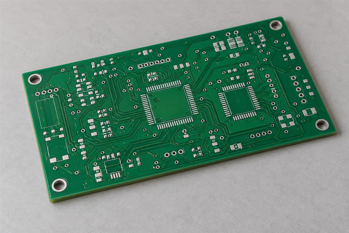
A bare PCB board is a fabricated printed circuit board before components are mounted. It already contains the designed copper interconnections and may include solder mask, markings and a protective finish on exposed pads. It is not simply a sheet of copper-clad material, and it is not an assembled circuit ready for a functional test.
Before sending bare boards to assembly, answer three questions: Is this the correct released design? Does the delivered board meet the agreed fabrication specification? Do the assembly files and components match it? A board can pass an electrical continuity test and still be the wrong revision for the parts waiting on your production line.
Recognize What a Bare PCB Order Actually Includes
A bare-board order normally delivers the physical interconnection platform, not the components, solder joints, firmware or a working electronic product. Confirm the scope in the quotation: a stencil, assembly service and test fixture should not be assumed to be included.
Think of the copper tracks as the fixed wiring. A pad is an exposed connection area where a component lead or terminal will be soldered. A via connects copper on different layers when its construction provides that connection. Solder mask is the usually colored coating around exposed connection areas; the white reference markings, when present, are the legend. Neither the board color nor the legend proves which laminate or copper thickness was used.
Not every visible hole has the same purpose. A plated component hole may carry both a lead and an electrical connection. An unplated mounting hole may be purely mechanical. Do not determine plating requirements from appearance alone: compare the hole definition and fabrication drawing.
| Item being supplied | What you are receiving | What still needs to happen |
|---|---|---|
| Copper-clad laminate | Insulating material with copper foil, before the required circuit pattern is fabricated | Fabrication of the circuit and specified features |
| Custom bare PCB | Your designed copper pattern, holes, outline and specified coatings or finishes | Component assembly and any required programming and assembly tests |
| Generic prototyping board | A predefined hole, pad or strip pattern | Your own wiring and component connections; it is not automatically your custom design |
| PCBA | A board with components assembled | Any testing, firmware loading or enclosure integration excluded from the agreed supply scope |
“Blank board” is an ambiguous purchase description because sellers may use it for either unprocessed laminate or an unpopulated patterned board. Send the design identifier and a clear deliverables list rather than relying on that phrase.
Turn the Board Description into an Agreed Specification
A usable specification combines the circuit data with the physical and manufacturing requirements. “Four-layer green PCB” leaves important questions unanswered: finished thickness, material designation, copper requirements, finish, hole tolerances and panel format are separate decisions.
Ucamco’s Gerber Job documentation explains that fabrication information extends beyond layer images to attributes such as material, finish and overall thickness. A job file can convey these attributes, but you still need to resolve missing or conflicting requirements with the fabricator.
| Confirm before fabrication | Put it in the release package | Do not infer it from |
|---|---|---|
| Design identity | Board number, revision, dated release manifest and approved exceptions | A familiar filename or an old photo |
| Construction | Layer order, agreed stackup, laminate requirements and finished thickness with tolerance | Green mask, visible edges or layer count alone |
| Copper | Required copper values and whether they refer to starting foil or finished copper, with the supplier’s interpretation confirmed | The word “1 oz” without context |
| Mechanical fit | Outline, slots, cutouts, finished hole sizes, plating requirements and critical tolerances | A copper-layer drawing or nominal dimension without a tolerance |
| Assembly surfaces | Surface finish, mask openings and any pad-specific requirements | Pad color or “lead-free” alone |
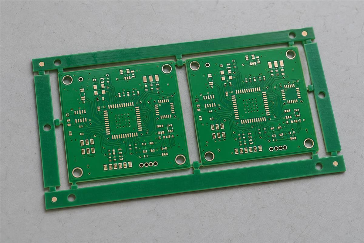
| Delivery format | Individual boards or an approved assembly panel, including rails and separation features where required | The fabricator’s manufacturing panel layout |
| Verification | Agreed acceptance criteria, electrical-test scope and any additional reports required by the design | A generic “QC passed” statement |
Use a Tolerance Example to Resolve Ambiguity
Suppose a drawing specifies a finished board thickness of 1.60 mm ±0.10 mm. The allowed interval in that example is 1.50–1.70 mm. A 1.74 mm measurement would be outside that interval, even if the order is casually called a “1.6 mm board.” This is an illustrative requirement, not a universal PCB tolerance.
Before rejecting or accepting the lot, verify the measurement location, instrument and agreed definition of finished thickness. If a connector or enclosure needs a tighter fit, address that before fabrication; an electrically correct board does not automatically fit the mechanical assembly.
For a controlled-impedance design, include the target, tolerance, relevant layer or structure and required verification. Layer count alone does not establish impedance. For fabrication-route details, see the separate bare PCB manufacturing process guide; the handoff task here is to establish which construction was approved and delivered.
Match the Bare Board to the Assembly Package
The board, parts list and placement data must describe the same released assembly. A complete set of files is not enough if those files belong to different revisions.
- Freeze one release. Identify the approved board revision, fabrication output, BOM, placement file and assembly drawing. Record any approved departures. Keep obsolete files out of the active production package.
- Match parts to footprints. For each critical component, compare the specified manufacturer part number and package drawing with the board’s land pattern. Check pin numbering and mechanical clearances; a similar package name is not proof of fit.
- Check orientation and side. Reconcile the placement file’s coordinates, rotation convention, reference origin and top/bottom interpretation with the assembler. Use a visual placement review, especially for polarized parts and fine-pitch devices.
- Agree the delivery panel. Review rail clearances, tooling requirements, fiducials, overhanging connectors and separation access with the assembler. A panel convenient for fabrication may not be suitable for the assembly equipment.
- Close discrepancies before scheduling assembly. Give unresolved items an owner and a written decision. Do not allow a verbal “probably the same board” to substitute for revision approval.
The BOM tells the assembler which parts to use. The CPL, or component placement list, describes where parts go and their orientation. The assembly drawing adds visual instructions and exceptions. Eurocircuits describes this cross-check between BOM, placement data and the bare-board layout in its assembly preparation guidance.
For example, revision B might change a connector footprint while an old revision A BOM remains in the release folder. The bare board can be perfectly fabricated to revision B, yet the supplied connector can still be wrong. The corrective action is a controlled file or component decision, not a request to rerun the bare-board electrical test.
Read Test Evidence Without Overestimating It
Bare-board electrical testing checks specified interconnections, typically looking for unintended breaks and connections. It does not establish that the eventual assembled product will perform its application correctly.
An open is an intended connection that is broken. A short is an unintended connection between conductors that should be separate. A net groups connection points intended to be electrically common. Eurocircuits’ electrical-test explanation illustrates this distinction. Its equipment choices and standard-service policies are supplier-specific, not universal requirements.
When reviewing evidence, ask which board revision and lot were tested, what reference data were used, what test scope and acceptance settings applied, and what happened to failed boards. Where the workflow supports it, clarify whether an independently exported design netlist was compared with the manufacturing data. A test against the wrong reference can give confidence in the wrong connectivity.
Keep these limits explicit:
- A continuity pass is not a controlled-impedance report. Request the specified impedance evidence separately when required.
- An electrical pass does not establish correct board thickness, hole fit, finish condition or component orientation.
- A visual check cannot verify all internal interconnections or buried features.
- A bare-board report does not replace assembled-board functional testing, programming or the product’s safety evaluation.
There is no single acceptance number suitable for every design and test method. Use the requirements agreed for the order and the applicable acceptance documents; ask the responsible engineer to resolve unclear criteria rather than inventing a pass/fail limit at receiving inspection.
Decide Whether to Release, Hold or Clarify the Lot
Release the lot when its identity, agreed evidence and assembly compatibility are confirmed. Hold affected boards when there is a mismatch or damage. Request clarification when information is missing; missing evidence is not proof that a physical board is defective, but it can prevent a justified release.
Bare-Board Handoff Checklist
- Board number, revision, purchase order and received quantity match the approved release.
- Lot identification remains linked to the received packaging and required supplier records.
- Critical outline, thickness, holes and slots are checked using the agreed receiving plan.
- Required test or conformity evidence identifies the correct design and lot.
- There is no unresolved visible damage, contamination, damaged packaging or suspect pad condition.
- The BOM, placement data, assembly drawing and supplied parts match the board revision.
- The panel format and component clearances are accepted by the assembler.
- Any exception has a documented engineering disposition before the affected boards enter assembly.
Use the supplier’s packaging, storage and handling instructions for the actual finish and material. Avoid touching solderable areas and keep identification with the boards when splitting a lot. If storage history is uncertain, seek an appropriate disposition; do not apply a generic baking temperature or shelf-life claim to every bare PCB.
When a discrepancy appears, record the lot, quantity affected, requirement, observation and evidence. For the thickness example above, that might be: “Drawing requires 1.50–1.70 mm; receiving measurements include 1.74 mm; affected quantity and measurement method attached; assembly paused pending review.” This gives the supplier a specific issue to investigate instead of an unhelpful “board quality is bad” complaint.
To discuss fabrication or assembly with PCBtry, send the released fabrication package, required stackup and finish, quantity, delivery format and critical acceptance requirements. Include the BOM and placement data if assembly is required. Use the contact page or email sales@pcbtry.com, and identify unresolved questions before asking for a firm production commitment.
Questions About Bare PCB Deliveries
Does “bare” mean there is no solder mask?
No. In this context it means components have not been assembled. A bare board can already have solder mask, legend and a surface finish. The order specification determines which are present.
Is a bare PCB the same as a copper-clad board?
Not usually. Copper-clad laminate is raw material. A fabricated bare PCB already has the required circuit pattern and manufactured features. Clarify the seller’s wording before buying.
Can I identify the number of copper layers by looking at the board?
Not reliably from an ordinary surface view. Use the approved stackup and manufacturing records. Do not mistake mask color or surface trace density for a layer-count measurement.
Do I need a BOM to order bare boards only?
A component BOM is normally for assembly and sourcing, not the core bare-board fabrication dataset. Special construction requirements still need to be communicated. Ask the fabricator which files its workflow requires.
Does a flying-probe pass prove the design will work?
No. The pass applies to the test performed against its reference and limits. Design correctness and assembled product performance require their own verification.
Can I accept a different surface finish if the board dimensions match?
Not automatically. Surface finish affects assembly compatibility and must match the order or an approved change. Ask the responsible engineer and assembler before accepting a substitution.
Should every bare board be baked before assembly?
No universal instruction is appropriate. Base any drying decision on the material, finish, packaging, storage history and qualified process instructions. Unnecessary or unsuitable heating can introduce problems.
What is the most important check when reordering?
Verify the released revision and approved exceptions before relying on the previous order. Then confirm that construction, finish, delivery panel and assembly data remain valid. “Same as last time” is not a substitute for an identified release.



0 Comments