
High frequency PCB design is an essential part of modern electronics. Whether you’re designing for 5G communication, satellite systems, or high-speed data processing, understanding the key elements of high frequency PCB design ensures a functional, reliable, and efficient product. Let’s walk through what makes high frequency PCB design unique and how to optimize its performance.
What is a High Frequency PCB?
A High Frequency PCB (Printed Circuit Board) is designed to handle circuits operating at frequencies above 1 GHz, commonly used in applications such as wireless communication, 5G, radar systems, satellite communications, and RF (Radio Frequency) circuits. HF PCBs are characterized by a low dielectric constant (Dk), low dissipation factor (Df), and minimal thermal expansion. These boards are specifically engineered to maintain signal integrity at high speeds, ensuring minimal signal loss, distortion, and interference.
What are the Challenges of High Frequency PCB Design?
Designing a high-frequency PCB comes with specific hurdles that need careful consideration:
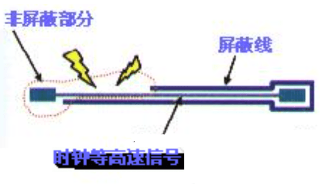
Electromagnetic Interference (EMI)
At high frequencies, PCB traces can emit or receive unwanted electromagnetic signals. EMI can distort signals, leading to poor performance, especially in communication systems. Proper shielding, trace layout, and grounding techniques can help reduce EMI, ensuring that signals are transmitted cleanly and without interference.
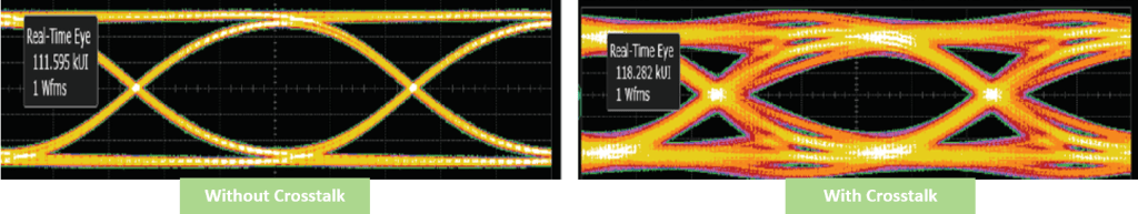
Signal Integrity
Signal integrity is crucial for high speed circuits. At high frequencies, signals can degrade due to reflections, crosstalk, and impedance mismatches. If not properly managed, these issues can cause data errors or loss. This is why precise impedance matching and proper routing are fundamental aspects of high frequency PCB design.
High Power and Heat Loss
High frequency circuits tend to generate more heat due to increased power consumption. Excessive heat can damage components, degrade performance, and reduce the lifespan of the PCB. Efficient thermal management, including the use of high-performance materials, is necessary to dissipate heat effectively.
What Are the Typical Materials Used for High Frequency Boards?
Choosing the right material is crucial for high frequency PCB design. The material affects the speed and efficiency at which signals travel across the board. Here are some common materials:
- FR4 (Standard PCB material): Though commonly used for lower-frequency circuits, it’s unsuitable for high frequency applications due to its higher dielectric constant and loss at high frequencies.
- PTFE (Polytetrafluoroethylene): Offers excellent dielectric properties and low signal loss, making it suitable for RF applications.
- Rogers: A brand of materials designed for high frequency applications with low loss and stable dielectric properties.
- Ceramic-based materials: Provide low loss and stable dielectric constant over a wide frequency range.
The choice of material impacts signal speed, integrity, and overall board performance.
High Frequency PCB Layer Stack-Up Design
The stack-up of a PCB refers to how the layers of the board are arranged. In high frequency PCB design, this is particularly important because the layer stack-up affects the board’s performance in terms of signal integrity and EMI control. Here are some considerations:
Minimize the Number of Layers
A key goal in high frequency PCB design is to reduce the number of layers as much as possible. Here’s why:
- Simplicity: Fewer layers simplify the overall design, reducing the complexity of routing and minimizing the risk of unintended interference between signal layers.
- Reduced Parasitic Effects: Each additional layer can introduce parasitic inductance and capacitance, which can degrade signal quality. Keeping the number of layers low minimizes these effects.
- Cost and Manufacturing: Fewer layers typically result in lower manufacturing costs and faster production times.
Use Controlled Impedance Layers
Impedance control is crucial for high frequency PCB design because it ensures that signals are transmitted without reflection, which could lead to data errors or signal loss. The idea is to match the impedance of the PCB traces to that of the source and load devices. Controlled impedance layers maintain consistent impedance across the board, ensuring that signals travel along traces with predictable characteristics.
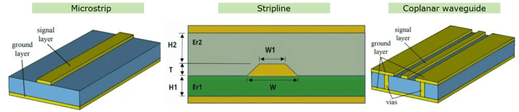
- Trace Width and Spacing: The width of the PCB traces and the distance between them play a critical role in maintaining controlled impedance. For example, microstrip traces (traces on an outer layer) and stripline traces (traces between two ground planes) have different requirements for trace width, distance from the ground plane, and the type of material used.
- Simulation: Advanced simulation tools can be used to model the impedance of the PCB traces, which helps designers fine-tune the stack-up for optimal signal transmission.
Strategic Use of Ground and Power Planes
Ground and power planes are essential in high frequency PCB stack-up design because they provide a low-impedance path for signals to return to the source, reducing noise and improving signal integrity.
- Ground Plane: The ground plane serves as the reference for all signals. It is typically placed directly beneath the signal layers and connected with multiple vias to reduce impedance variations. A solid, uninterrupted ground plane helps reduce EMI and crosstalk between adjacent signal traces.
- Power Plane: A dedicated power plane supplies a clean and stable voltage to the components. This plane helps minimize voltage fluctuations and power noise, which can affect the performance of sensitive high-frequency components.
- Plane Proximity: Placing the signal layers near the ground and power planes minimizes the path for current to travel, reducing inductance and noise. This layout also improves return current paths, which is crucial for maintaining high-speed signal integrity.
- Decoupling Capacitors: These are often added near the power and ground pins of ICs to filter out high-frequency noise and smooth out any voltage fluctuations. Proper placement is essential for effective decoupling.
The layer stack-up design is one of the most critical aspects of high frequency PCB design. By carefully selecting materials, minimizing layer count, controlling impedance, and optimizing the placement of ground and power planes, a designer can ensure optimal performance in terms of signal integrity, EMI control, and overall efficiency. Proper stack-up design minimizes issues like noise, interference, and power loss, ensuring that high frequency circuits perform at their best.
Tips for Designing High-Frequency PCBs
A high frequency PCB is only as good as its design. Let’s go over a few tips to ensure your design delivers the best performance possible:
Keep Loop Area as Small as Possible
A smaller loop area reduces the inductance and electromagnetic radiation. Minimizing loop area is especially important in high frequency designs, as it helps prevent EMI and ensures that signals maintain integrity.
Take Your Time to Decide the Type of Transmission Line
There are various types of transmission lines used in PCB designs, including microstrip, stripline, and coplanar waveguide. Each has its advantages and disadvantages, and selecting the right one for your application will help improve performance.
Maintain Accurate Impedance Matching
Impedance matching is essential for minimizing signal reflections and ensuring smooth transmission of high-frequency signals. Accurate impedance control can be achieved by adjusting the width of traces, the distance between traces, and the use of ground planes.
Do Not Use FR4 for High-Frequency Applications
As mentioned earlier, FR4 is not suitable for high-frequency applications due to its higher loss and poor signal propagation at high frequencies. Use materials like PTFE or Rogers that offer better performance at high frequencies.
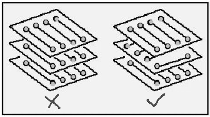
Adopt Orthogonal Routing While Directing a Signal on Different PCB Layers
Routing signals orthogonally (at right angles) between layers reduces crosstalk and interference. It also helps ensure that the signal maintains its integrity as it transitions between layers.
Always Check the Highest Frequency Net and Evaluate the Fastest Rise Time in the System
The highest frequency net dictates the overall performance of the PCB. By evaluating the rise time of the system, you can optimize the design to handle high-speed signals without distortion.
Check the Electrical Specifications at the Inputs and Outputs of the Sinks and Sources
Properly matching the electrical specifications of inputs and outputs ensures that signals remain stable and perform well across the board. Incorrect matching can lead to signal degradation or even component failure.
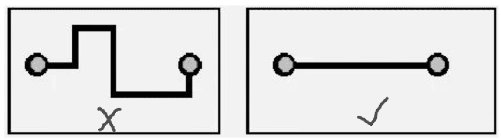
Using Shorter Trace Lengths
Shorter trace lengths reduce the signal travel time and minimize the risk of signal degradation or EMI. It also reduces the potential for reflections in high-frequency signals.
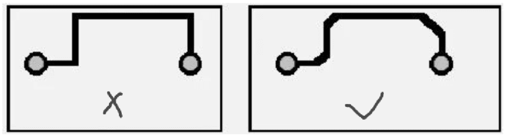
Avoid Sharp Bends
Sharp bends in PCB traces can cause impedance mismatches and signal reflections. To avoid this, use gentle curves and keep the trace width consistent.
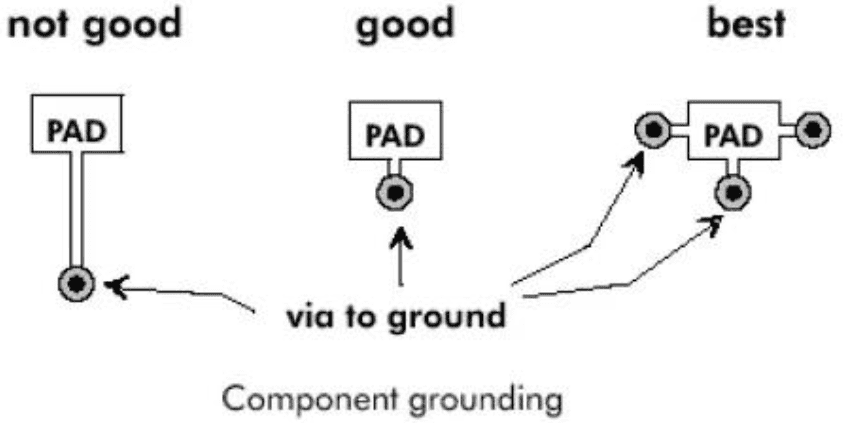
The Right Grounding
A solid grounding system ensures that high-frequency signals have a low impedance path to return. This helps minimize noise and signal degradation. Make sure to use multiple ground planes where possible and minimize the distance between the return paths and the signal traces.
Via Placement
Vias are necessary for connecting different layers of the PCB, but they add inductance and capacitance to the circuit. Use fewer vias and ensure they are strategically placed to minimize any negative effects. High-frequency signals are sensitive to the layout and placement of vias and traces:
- Via Minimization: Vias add inductance and capacitance, which can distort signals. Minimizing the number of vias, especially for high-frequency traces, is crucial.
- Via Types: If vias are necessary, blind or buried vias (vias that do not go through the entire board) are preferable because they can reduce signal loss.
- Via Placement: Vias should be placed as close to the signal trace as possible to minimize signal degradation.
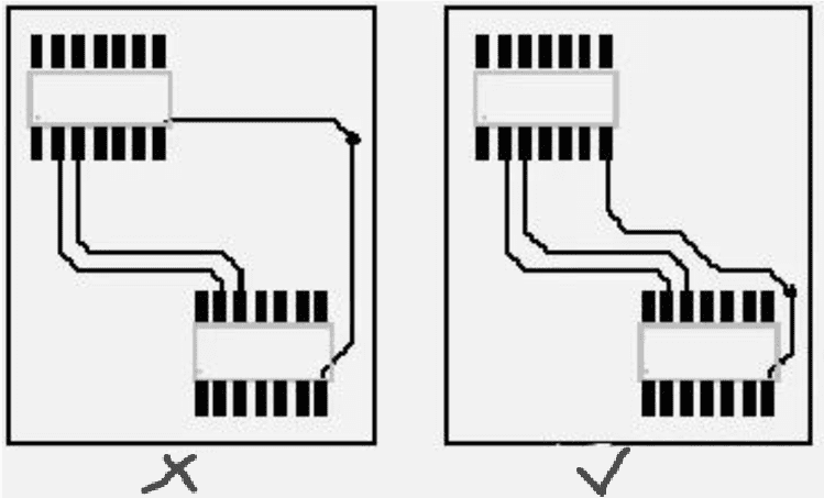
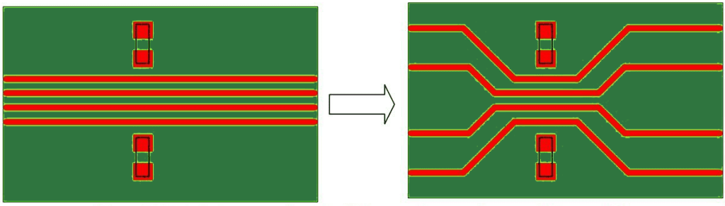
Differential Pair Routing
For high-speed signals, differential pair routing is essential. It ensures that the signal and its return path travel close to each other, reducing noise and ensuring that the signals arrive in phase.
Implement Shorter Leads Between the Pins in a High-Frequency Circuit
Minimize the distance between components to reduce parasitic inductance and capacitance. This helps improve signal integrity and reduces the risk of EMI.
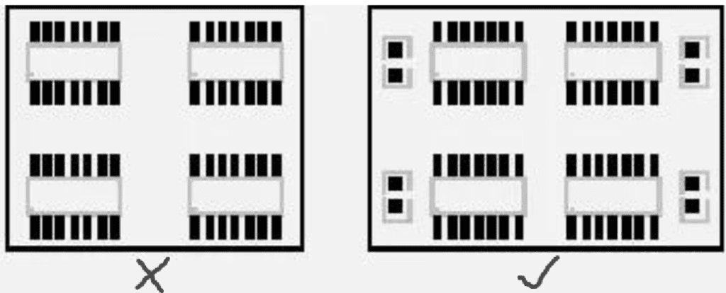
Add More Spacing Between Adjacent Signal Lines and Minimize the Parallel
Maintaining proper spacing between adjacent signal traces helps reduce crosstalk and interference. It also allows signals to propagate more effectively.
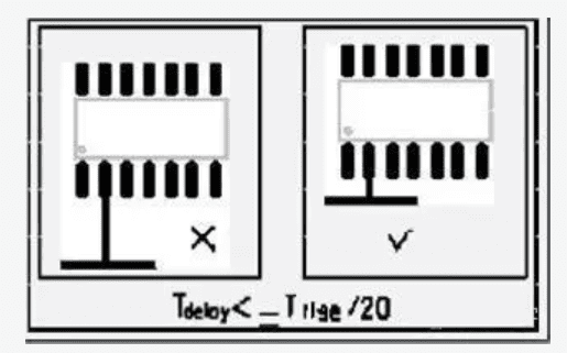
Add Decoupling Capacitance as Near as Possible to the Supply and Ground Pins
Decoupling capacitors help stabilize the power supply voltage and prevent noise from entering the system. Place them as close as possible to the power and ground pins to maximize their effectiveness.
Testing and Validation in High Frequency PCB Design
Once your high frequency PCB design is complete, testing and validation are crucial to ensure that it works as intended. Use specialized tools like network analyzers and oscilloscopes to test for signal integrity, impedance matching, and overall performance. Performing these tests under real-world conditions will help identify potential problems before mass production. If issues arise, iterate on your design and re-test until you achieve the desired performance.
Conclusion: High frequency PCB design is a challenging yet rewarding aspect of modern electronics. With the right materials, stack-up design, and attention to detail in routing, grounding, and impedance matching, you can create a board that performs at its best. By following these tips and understanding the challenges, you’ll be well on your way to designing high-frequency PCBs that meet the demands of the most sophisticated applications.
If you require professional PCB design services or consultation, or if you have any further questions, Thindry PCB is here to assist you.


0 Comments