




Solder balling after reflow is unintended solder left outside the joint. Start by locating it: scattered fine spheres suggest a different investigation from a large bead beside a chip component or a continuous bridge between pads. Photograph the defect, compare the printed deposits and placed parts, then check the paste lot and measured board-temperature profile. Increasing the oven setting before those checks can hide the cause or create another defect.
The guide below covers external balls and beads on SMT assemblies, not the intentional solder balls under a BGA. Its comparison table and trial worksheet help separate a material problem from a printing, placement or heating problem.
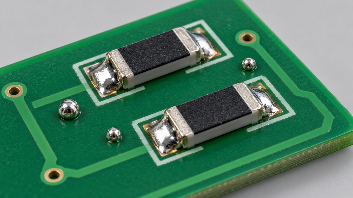
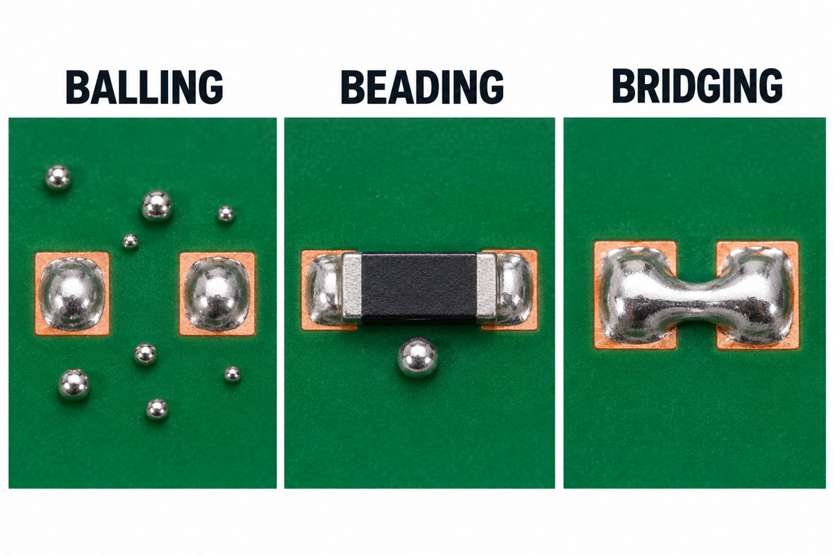
Solder balling vs solder beading vs bridging: what is the difference?
The location and shape tell you where to start, but do not prove the cause. A bead beside the middle of a resistor is not the same observation as powder-like spheres across the solder mask.
| Observation | Working classification | First evidence to collect |
|---|---|---|
| Separate small spheres away from the main joint | Solder balling | Location map; paste outside pads before heating; material and profile history |
| One or a few larger beads beside the middle of a chip | Mid-chip beading | Paste volume and location beneath the component; aperture and placement comparison |
| Continuous solder joining conductors that should be separate | Bridging | Inspect the actual connection and isolate power before further testing |
| Granular deposit that has not formed a sound joint | Incomplete coalescence or wetting problem, possibly with balls | Measured thermal history and a controlled fresh-material comparison |
Tecan’s stencil handbook distinguishes near-pad balls, poor wetting with balling, and mid-chip beads. Treat these patterns as investigation branches rather than interchangeable names.
What causes solder balls after reflow?
Look for evidence of misplaced paste, material deterioration or an unsuitable thermal cycle. Several causes can coexist on one board.
- Near-pad balls: inspect print alignment and the seal between stencil and board. Paste deposited outside the intended land may remain isolated.
- Chip-side beads: examine whether excess paste has been pushed beneath the body. Paste trapped there may not return to the terminations during reflow.
- Scattered balls: investigate moisture exposure, rapid volatile release and powder oxidation rather than assuming insufficient peak temperature.
- Balling with poor wetting: compare the whole thermal cycle with the material requirements. An extended soak can consume the useful process window.
The mechanism checks above draw on Tecan and Kester’s defect-minimization guide. Neither makes a photograph alone a root-cause test. Keep a suspect board unchanged until its defect locations and process records are captured.
How do you stop solder balls without changing everything?
Use a controlled comparison that follows the board through printing, placement and reflow. The following investigation sequence is a practical worksheet, not a validated recipe for every assembly.
- Contain and label. Separate suspect assemblies. Record board revision, panel position, reference designator, paste lot and when the issue first appeared.
- Inspect the print. Compare an affected location with a good location before placement. Record deposit shape, offset and measured volume where SPI is available. Check stencil underside cleanliness and board support.
- Inspect after placement. On a designated trial sample, compare paste spread before and after placement. Review the programmed component height and placement force with the equipment owner; do not select a universal force value.
- Check material traceability. Verify alloy, formulation, expiry and handling against the actual supplier document. A fresh approved lot is a more useful comparison than adding an unknown thinner to suspect paste.
- Measure the board profile. Use a representative populated profiling assembly. Relate the recorded temperatures to the affected locations and the paste and component limits.
- Change one justified factor. For example, correct a verified print offset while retaining the same paste and profile. Repeat the observation at the same locations. If defects fall but joints become insufficient, the trial has not passed.
For paste squeezed under chip bodies, Indium’s no-clean transition example supports reviewing aperture geometry and paste volume. Discuss a localized home-plate or other reduction with the stencil supplier; do not shrink every aperture by an arbitrary percentage. Check both bead reduction and joint formation.
Which Kester EP256 parameters matter when investigating solder balls?
Use the exact formulation and test conditions, not the brand name alone. EP256 is a documented example of how to read paste specifications, not a claim that PCBtry uses or stocks it.
| EP256 reference | Published value or condition | How to use it |
|---|---|---|
| Part 41500014 | Sn63Pb37, Type 3, 25–45 µm, 500 g jar | Confirm the ordered alloy and powder; this is leaded material |
| TDS physical-property sample | Sn63Pb37, 90% metal, −325/+500 mesh | Do not apply the reported properties to every EP256 variant |
| Typical viscosity | 1,400 poise; Malcom viscometer, 10 rpm, 25°C | A different method or temperature is not a like-for-like comparison |
| Typical initial tack | 40 g; Kester method 1W-QC-3-04 | Not a component-placement force setting |
| Solder-ball test | Pass; J-STD-005 / IPC-TM-650 2.4.43 | Material test result, not proof that your assembly will be ball-free |
| Storage and shelf life | 0–10°C; six months from manufacture with proper handling | Check the lot label and current supplier instructions |
Sources: Kester product listing and EP256 technical data sheet. Typical values are not guaranteed tolerance limits; none is invented here. The SnPb example is not a lead-free substitution recommendation.
Should you increase temperature or extend the soak?
Only after a measured profile shows what needs correcting. An oven or hotplate display is not the temperature history of the solder joint. A higher setting does not tell you whether the flux activated correctly or whether a cold location reached its required conditions.
Indium’s ramp-rate guidance explains why controlled heating helps volatile release. Conversely, simply making heating slower is not always helpful: excessive exposure can impair the flux’s useful action. Compare ramp, soak if used, time above liquidus and peak against the specific paste instructions and component limits together.
Do not transfer an SnPb curve to SAC or a low-temperature bismuth paste. Kester’s lead-free defect discussion also emphasizes alloy-appropriate flux behavior and hot slump. Start with the approved material profile, not a temperature copied from a forum. The broader PCB reflow process guide provides the process context; this investigation stays focused on stray solder.
Can you remove solder balls and release the board?
Removing a visible ball is containment, not evidence that the process or assembly is acceptable. No-clean describes a flux system; it does not mean unwanted metal can automatically remain.
Keep power off during inspection and use an approved rework or cleaning procedure compatible with the assembly. Do not blow particles toward connectors or underneath packages. After removal, inspect the surrounding joints and possible hiding locations, then complete the required electrical and functional checks. Where access or workmanship is uncertain, hold the board for qualified review against the applicable customer requirements.
Record whether particles were loose, embedded in residue or attached to a joint. That observation matters to the investigation, but this article does not assign an IPC class, a universal allowable ball count or a safe particle diameter. For cleaning-method boundaries, consult the post-soldering PCB cleaning guide.
What should you record before the next assembly run?
Keep a before-and-after record that identifies the changed factor and checks for new defects. This makes the next trial reviewable instead of relying on “it looked better.”
| Record field | Baseline | Trial and release evidence |
|---|---|---|
| Board and location | Revision, panel position, reference designator, photograph | Same inspection locations and magnification |
| Print and placement | Aperture revision, deposit data, visible paste displacement | Changed setting or geometry; joint and bead observations |
| Material | Supplier, exact paste, alloy, lot, expiry, exposure record | Same lot or explicitly identified approved replacement |
| Thermal cycle | Measured profile, probe locations, load condition | Updated trace; paste and component limits checked |
| Decision | Defects counted per inspected boards or locations | Equivalent denominator, other defects, test result and reviewer |
Use the same denominator when comparing trials. Five defects on ten boards cannot be compared directly with five defects on a hundred boards. A small trial is screening evidence, not an automatic production-yield guarantee.
Solder balling after reflow FAQ
Will more heat make tiny solder balls join together?
Not reliably. Establish whether the deposit failed to reflow, wet poorly or was already separated from the pad. Measure the board profile before changing it; extra heat cannot correct a misplaced deposit and may damage the assembly.
Can using paste straight from the refrigerator cause problems?
Follow the formulation’s warm-up instructions before opening and printing. Avoid introducing condensation. The EP256 example calls for stabilization at room temperature; it does not justify one fixed warm-up time for all containers or pastes.
Can old paste cause balling even when it still looks usable?
Appearance alone does not establish suitability. Check its documented life and handling, then compare with an approved in-date lot under controlled conditions. Do not extend production use solely because an online user reported success with expired paste.
Should I add extra flux to fix the problem?
Do not treat unqualified flux addition as a production correction. It changes the material system and residue. An approved rework process is a separate decision from solving a recurring print or reflow defect.
Are balls trapped in no-clean residue harmless?
Do not assume so. Assess unintended metal independently from the residue classification. Document its location and attachment, and use the applicable assembly acceptance requirements rather than appearance alone.
Why do beads appear beside resistors rather than at their ends?
Investigate paste displaced beneath the body, especially when the pattern repeats at the same component style. Compare pre-placement deposits, aperture geometry and placement settings before blaming the oven.
Why do I see balls when using hot air?
A localized heat source adds another process variable. Record the actual board response and paste placement; do not infer joint temperature from the tool display. Use the same material and defect-pattern checks as for oven reflow.
Should every stencil aperture be made smaller?
No. A global reduction can trade beads for insufficient solder. Target the affected geometry, consult the stencil supplier, and verify transfer and finished joints before accepting the change.
Need an assembly review? Send PCBtry the board revision, Gerber and paste layers, BOM/CPL, paste specification, defect photographs and available profile/SPI records through the contact page. Identify whether you need a new-build quotation or help evaluating a recurring assembly issue.



0 Comments