




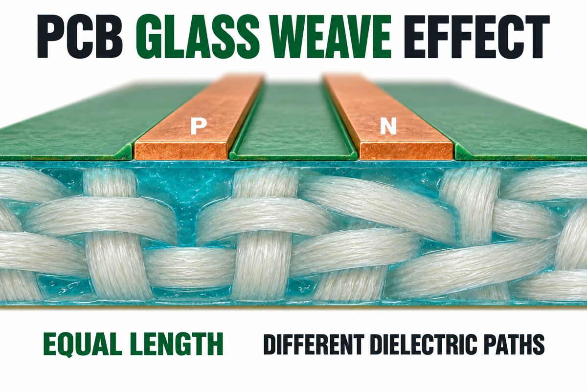
The PCB glass weave effect is a local change in a trace’s dielectric environment as it passes over glass bundles and resin-rich gaps. Two equal-length traces can therefore have different delays. The practical response is to review the actual laminate construction, routing direction and channel timing budget together, not to add length compensation based on a generic FR4 number.
This matters when a differential channel has little timing margin or a long route that repeatedly follows the weave. It is not a reason to buy an expensive laminate for every board. Start with the interface requirements and determine whether the fabrication information is detailed enough to support your design assumptions.
Why can equal-length PCB traces have different delays?
Length matching controls geometry; it does not make the material beneath both conductors identical. Imagine two runners covering the same distance on different surfaces. In a PCB, the relevant difference is electromagnetic propagation through the surrounding dielectric, not mechanical friction. The field around each trace samples both resin and reinforcement. If the two traces sample these regions differently, their arrival times can differ.
A Reddit discussion about prepreg selection illustrates the purchasing problem: a designer knows glass-style numbers but cannot tell whether they guarantee uniformity along the pair. They do not constitute a complete electrical specification. Resin system, resin content, construction and orientation still matter. For the broader distinction between a material property and a trace model, see our FR4 dielectric-constant guide.
Keep two checks separate: intra-pair skew is the delay difference between the two conductors of one pair; inter-pair timing concerns different pairs. Use the exact interface specification for each. A loss problem, a via discontinuity and a skew problem can all reduce margin, but they do not have the same remedy.
Spread glass vs angled routing: which approach should you choose?
Material selection changes the dielectric structure; routing changes how the traces sample that structure. They are complementary controls. Neither should be described as a universal cure. Compare feasible options with the fabricator before locking the board outline, layer assignments and routing rules.
| Option | What it changes | What must be confirmed |
|---|---|---|
| Spread-glass construction | Distribution of glass bundles and resin-rich gaps | Actual grade and construction; electrical model and available thickness, not just a marketing description |
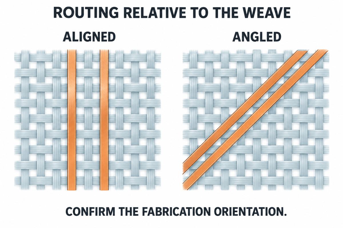
| Angled routing | Track direction relative to the weave | Fabrication orientation and effects on spacing, reference continuity and route length |
| Fabricator image rotation | Board image orientation on the material panel | Documented angle and reference direction, panel utilization and approval before CAM release |
| Zig-zag routing | Local track traversal across different dielectric regions | Added geometry, coupling and discontinuities; no arbitrary amplitude or pitch |
TI’s High-Speed Interface Layout Guidelines, Rev. J, section 2.1 discusses image rotation, angled tracks and zig-zag routing. Its illustrated rotation guidance is 10-35 degrees relative to the weave. Treat that as application-note guidance to evaluate, not a guaranteed angle for every interface. The weave direction, not the drawing border alone, is the reference.
Do not simultaneously assume that the fabricator will rotate the image and that your routing angle already represents the final relative angle. Put the intended relationship on the approved stackup or fabrication notes. A change that improves one long route may complicate fanout or the panel; review the whole implementation.
Isola I-Speed constructions: which real parameters matter?
Specify a construction, not merely a laminate family or glass-style number. The following examples come from the core-construction table on Isola’s current I-Speed product page. They are manufacturer information, not measurements from PCBtry or guaranteed finished-board values.
| I-Speed core construction | Listed resin / thickness | Listed electrical values at 10 GHz |
|---|---|---|
| 1 x 1067 | 66.00% resin; 0.0020 in / 0.051 mm | Dk 3.57; Df 0.0059 |
| 1 x 3313 | 52.00% resin; 0.0035 in / 0.089 mm | Dk 3.89; Df 0.0061 |
Dk and Df are dimensionless. These rows identify different core builds; they are not an equal-thickness experiment isolating weave style. The construction table does not state a per-row tolerance or test method. Request the applicable characterization and agreed manufacturing tolerances rather than inventing them. Do not use core thickness as the finished pressed thickness of a prepreg layer. Nor does either row provide a guaranteed differential-skew limit.
The official page also records removal of the low-Dk glass option in revision C. Older downloadable material descriptions may not match the current offering. Confirm the current grade, construction and availability for the purchase; a previously saved PDF is not evidence that an option is still supplied. PCBtry availability requires project-specific confirmation.
How should you review glass-weave risk before routing?
Start with a timing requirement, then ask whether the material and route can be evaluated against it. Do not begin by choosing a correction length. An unknown physical offset between copper and reinforcement cannot be reliably canceled by guessing which conductor will be slower.
- Identify the constrained channel. Record the interface, transmitter and receiver, relevant vendor guidance, longest routes and permitted skew. Do not confuse total channel delay with the difference inside a pair.
- List the other asymmetries. Include packages, breakouts, layer transitions and connectors. Correct known geometry problems before blaming the weave.
- Get an actual build proposal. Ask for material grade, each core/prepreg construction, pressed thickness assumptions, copper and orientation. Hold unresolved substitutions for review.
- Compare feasible mitigations. Evaluate material and routing choices with the approved impedance geometry. Confirm that the change does not introduce a reference-plane interruption or uncontrolled detour.
- Define the evidence needed for release. Agree on channel modeling or measurement, fixtures, test structures and acceptance criteria. Preserve the approved build with the results.
For an illustrative budget exercise, suppose a project allocates 5 ps to residual board intra-pair skew and its analysis predicts 7 ps for the proposed build. That proposal fails this assumed allocation even if the CAD length check passes. These are example numbers, not measured material values or a standard limit. The decision is to revise the build or routing and reassess, not quietly change the pass criterion.
What should a glass-weave stackup checklist include?
Make every assumption traceable to a revision and an owner. Use this record when comparing quotations or transferring a prototype to production. Blank cells should become questions before fabrication, not undocumented assumptions.
| Record | Evidence to retain | Reason to hold release |
|---|---|---|
| Material identity | Manufacturer, grade, construction and current data revision | Only “FR4” or an unapproved equivalent is specified |
| Layer geometry | Core/prepreg build, pressed dielectric dimensions, copper and impedance model | Values refer to a different construction or frequency |
| Orientation | Defined weave reference and approved board-image/routing relationship | Supplier and designer use different angle references |
| Timing requirement | Named interface requirement and board allocation | Length matching is the only pass criterion |
| Verification | Representative model or measurement, setup and acceptance limits | An impedance result is presented as proof of every timing requirement |
| Change control | Approved substitutions and revalidation responsibility | Material, layer construction or orientation changes without review |
A coupon answers the question it was designed and measured to answer. An impedance coupon passing its specified tolerance is useful, but that alone does not establish the delay difference along every routed pair. Choose verification that represents the risk, and make the required report part of the order rather than an afterthought.
What if a length-matched channel still fails?
Preserve the failing conditions and investigate competing causes. Record board lot, stackup revision, lane, operating conditions and measurement setup. Check whether the result repeats on the same board and changes across boards. Compare connectors, transitions and return paths before assigning the failure to material nonuniformity.
A useful comparison holds the rest of the channel constant while changing one controlled factor. If both material and routing change, a better eye diagram does not identify which change helped. Avoid tuning one board into compliance with an undocumented length offset that may not transfer to the next panel. For a high-speed PCB, agree on the evidence and manufacturing controls before ordering the next build.
PCB glass weave effect FAQ
Does length matching eliminate glass-weave skew?
No. It removes a known geometric mismatch, but local dielectric differences may remain. Keep the CAD check and the electrical timing check separate. A successful length rule is necessary where specified; it is not proof that the entire channel meets its timing requirement.
Is 1080 glass always unsuitable for high-speed routing?
No universal rejection follows from the style number alone. Review the resin system, construction, route and interface budget. Ask the fabricator for the actual build rather than ranking every 1080-based material below every alternative without matching conditions.
Will two prepreg plies cancel the weave effect?
Do not assume cancellation. The relative placement of the reinforcement and the fields around the traces must be considered. A two-ply construction can be evaluated, but it needs its own stackup model and fabrication information rather than an automatic pass.
Are 2116 and 3313 interchangeable?
Not as uncontrolled substitutions. The construction, resin content and dielectric thickness can change along with the style. Review the proposed replacement against the approved electrical and mechanical requirements, and document acceptance before the shop builds it.
Should every pair be routed at 45 degrees?
No. An angle relative to the board outline does not establish an angle relative to the weave. Confirm the material orientation and applicable device guidance. Check the resulting geometry and panel plan instead of treating a familiar CAD angle as a universal solution.
Can I add a small zig-zag everywhere?
Only after evaluating the resulting route. Added length and geometry may introduce other problems. The SFP+ community discussion raises exactly this concern; an unverified fixed amplitude from a comment should not become a production design rule.
Does a low Df guarantee low skew?
No. Df concerns dielectric loss; it does not specify spatial uniformity or the timing difference between two conductors. A material can help one part of the channel budget without resolving another. Ask for the data relevant to the actual failure mechanism.
Does a passing impedance coupon prove the pair is safe?
It proves only the measured structure met its defined impedance criterion. It does not automatically prove skew, mode conversion or the complete channel margin. Define a representative verification plan appropriate to the interface and retain the build and test records together.
What should you send for a stackup review?
Send the fabrication data, board outline, proposed stackup, critical layer assignments, impedance targets, longest differential routes and the interface timing requirements. Include any required laminate grade, orientation or substitution restrictions, plus the desired qualification reports. For an existing failure, add the board lot and repeatable measurement conditions.
Contact PCBtry or email sales@pcbtry.com to request a project-specific stackup and manufacturing review. Ask the team to confirm material availability, the agreed build and verification scope. The useful outcome is an approved set of assumptions that design and fabrication share, not an unsupported promise of zero skew.



0 Comments