




What does PCB appearance inspection actually establish?
The PCB appearance inspection process checks the visible condition of an unassembled board against its released drawing and agreed acceptance requirements. It connects an observation to a decision: accept the inspected feature, hold it for further evaluation, or record a confirmed nonconformance. A neat-looking board is not proof of complete electrical or structural quality.
This guide concerns bare boards, before components are fitted. The public IPC-A-600K scope excerpt distinguishes externally and internally observable conditions. Internal evaluation can require specimen preparation such as microsectioning. The excerpt explains the scope; use the full standard and revision specified for your order for actual acceptance decisions.
| Question | Appearance inspection can contribute | What it cannot establish alone |
|---|---|---|
| Does the board match the order? | Visible identity and feature comparison | Every hidden layer or material property |
| Is a surface feature damaged? | Location and visible extent of an anomaly | Its full depth or long-term effect |
| Is an opening obstructed? | A visible obstruction requiring review | All internal plated-hole conditions |
| Can the lot ship? | Completion of the appearance portion of release | Completion of all other contractual tests |
Keep the wider PCB testing process separate. This article does not replace continuity, isolation, dimensional or material verification. Its purpose is to make the visual inspection decision reproducible rather than subjective.
What must be ready before inspection starts?
Start with a defined acceptance basis, an identifiable board and an observation setup that reveals the feature. Otherwise, two inspectors can examine the same board and legitimately reach different conclusions because they are using different references.
- Identity: part number, drawing revision, lot or panel identifier and inspection stage.
- Requirements: released fabrication drawing, applicable standard and revision, agreed class where relevant, and customer-specific appearance conditions.
- Coverage: inspected surfaces and features, sampling or full-inspection scope, and any inaccessible areas.
- Equipment: suitable illumination, viewing equipment and calibrated measurement tools when a dimension determines acceptance.
- Disposition: who may accept, request more evidence, authorize permitted work or approve a documented deviation.
Use lighting that makes the relevant feature observable without glare hiding it. If changing the viewing angle makes a bright mark disappear, do not immediately call it damage. Inspect again under controlled conditions. A phone photograph can preserve an observation, but its zoom level is not automatically a calibrated measurement.
Do not select one universal microscope magnification or scratch-size limit from an unrelated example. The applicable requirement and feature determine the inspection method. Similarly, a customer-approved reference sample helps communication but must not silently override a drawing or governing requirement.
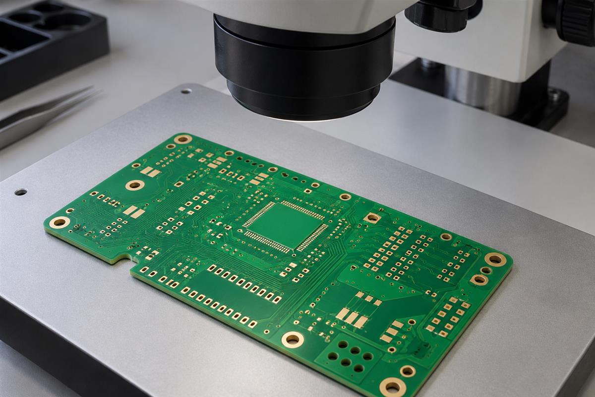
How does the PCB appearance inspection process work?
Follow a consistent route from identity to observation, evidence and disposition. Keep accepted boards and unresolved boards physically and administratively separate so an uncertain finding cannot disappear into the shipping quantity.
Step 1: Verify the board and the inspection basis
Match the physical board to the released order before spending time on small surface marks. A perfect-looking wrong revision is still the wrong product. If the identifier is missing or inconsistent, place the board on hold and reconcile the traveler, drawing and production record. Record the reference revision used so a buyer can later reconstruct the decision.
Step 2: Survey both faces and the accessible perimeter
Use a repeatable viewing route, such as one face, the perimeter, then the other face. This is a suggested work sequence, not an IPC-mandated scan path. Control handling so the inspection does not introduce damage or contamination. Confirm expected visible features against the drawing rather than relying on memory.
Eurocircuits’ published final-inspection description includes checks of cosmetic condition, mask, markings, holes and board features. Its specific sampling rules and numerical limits belong to its stated process; they are not universal PCBtry acceptance limits.
Step 3: Examine suspicious features without changing them
Locate the finding before cleaning, scraping or touching it. Save an overview showing where it is, then a detail view. Altering a suspected mark too early can remove evidence or create a new defect. If cleaning is appropriate, use an approved procedure and record before-and-after condition; do not improvise with a solvent or abrasive.
| Observation area | Useful question | Escalation when appearance is insufficient |
|---|---|---|
| Pad and surrounding mask | Is the observed opening consistent with the released design? | Compare the controlled mask/copper data and applicable acceptance criterion |
| Mark or scratch | Where is it, and which feature may be affected? | Measure or evaluate the affected feature; do not assign a universal scratch allowance |
| Hole or slot | Is the visible opening as expected? | Use the required dimensional or structural inspection if fit or internal condition is uncertain |
| Finish or discoloration | Is this a lighting effect, residue or a persistent anomaly? | Request the appropriate material, finish or solderability evaluation where required |
| Edge and identification | Is the outline intact and identity traceable? | Check the drawing or production record before release |
Step 4: Compare evidence with the actual criterion
Record the requirement used, not just “looks bad.” A visible difference is a finding; it becomes a confirmed nonconformance when evidence shows the applicable requirement is not met. If the criterion is unclear or the observation cannot resolve it, use a hold status and seek qualified review. That prevents both unnecessary scrap and unsupported acceptance.
Step 5: Close the decision and recheck affected work
Document the authorized outcome. If permitted cleaning, repair or other work is performed, identify the affected boards and complete the required reinspection and any related retest before release. Repeated findings should return to the process owner for investigation; sorting the lot alone does not explain why the issue occurred.
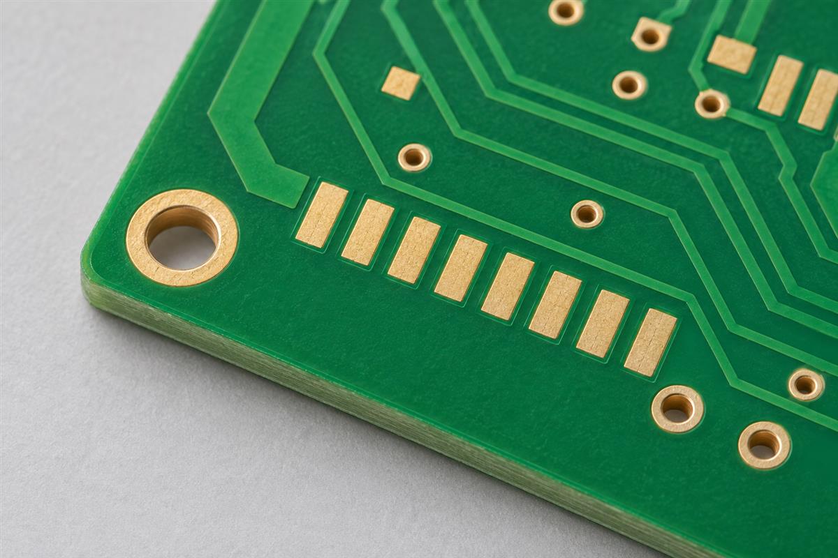
How should you record and resolve a doubtful finding?
Make the record useful to someone who was not at the bench. The minimum practical record links identity, location, evidence, requirement and decision. It should distinguish the observer’s description from an unproven cause.
Example: an inspector sees a pale line beside a connector pad. “Board scratched, reject” skips several questions. A better initial record says which board and side, which connector location, whether the line crosses a conductive feature, and which images preserve it. The board stays on hold until the relevant criterion can be evaluated. The example is a reasoning exercise, not a defect diagnosis from a photograph.
| Record field | What to enter | Why it matters |
|---|---|---|
| Identity and location | Part/revision, lot/panel/board, side and feature reference | Another person can find the same place |
| Observation | Neutral description, overview and detail image, scale when needed | Separates visible evidence from guessed cause |
| Evaluation basis | Drawing note or agreed criterion and any measurement method | Makes the pass/hold/fail reasoning checkable |
| Containment | Which units are held and how they are identified | Prevents accidental mixing with released boards |
| Closure | Reviewer, decision, authorized action and reinspection result | Shows who released the uncertainty and on what evidence |
For example, if three boards in an inspected sample of twenty show a similar mark, report exactly that observation. Do not claim that 15% of the entire lot is defective, or that all remaining boards are acceptable. The agreed sampling and escalation plan controls the next step. If no such plan exists, keep release unresolved while it is established by the responsible parties.
What belongs in the shipment release package?
The release package should connect the appearance result to the shipped units and show that open findings are closed. A single attractive photograph or an unsigned “visual pass” statement is weak evidence.
- Part number, revision and lot identity matching the shipment.
- Inspection scope, reference requirements and actual coverage.
- Recorded exceptions, their disposition and required approvals.
- Reinspection results after any permitted work.
- Other required test results, kept distinct from the visual inspection result.
- Release authority and quantity reconciliation.
Before PCB assembly, make unresolved bare-board findings visible to the responsible manufacturing and quality teams. Do not let component loading turn an inexpensive clarification into a difficult assembled-board investigation.
Frequently asked questions
Is appearance inspection the same as AOI?
No. Appearance inspection is an inspection purpose and decision process. Automated optical inspection is one possible tool. The program, coverage and review criteria still need definition.
Does a visible scratch always mean rejection?
No universal decision is justified. Its location, affected feature and applicable acceptance requirement determine the evaluation. Hold doubtful cases for review.
Can a photograph prove copper thickness?
An ordinary surface photograph cannot establish the required thickness. Use the specified measurement or structural evidence.
Should every board be visually inspected?
Define coverage in the inspection plan and purchase requirements. Do not silently change between sampling and full inspection or infer one from a supplier’s generic quality statement.
Is a darker surface automatically defective?
No. Lighting and surface condition affect appearance. Establish the observation and applicable requirement before assigning a defect or accepting it.
May an inspector repair a questionable area?
Only through the authorized procedure and scope. A finding does not itself authorize repair, and repaired work requires the specified verification.
Does a clean appearance prove absence of contamination?
No. Some contamination is not visibly detectable. If cleanliness testing is required, a visual pass is not a substitute.
What should a buyer send when disputing a finding?
Send the board and lot identity, location, original images, applicable drawing requirement, inspection method and requested decision. Avoid debating a cropped image with no traceability.
To agree the inspection scope before fabrication, contact PCBtry with the released fabrication package, acceptance requirements, critical appearance areas, quantity and requested reports. Ask which checks and evidence are included, and resolve exceptions before placing the order.



0 Comments