




What materials can a PCB laser marker process?
PCB laser marking can be developed for solder-mask surfaces on FR4 boards, exposed polymer surfaces such as polyimide, and ceramic substrates. Selected metal surfaces can also be marked with an appropriate system. These are candidate material families, not a guarantee that one laser or one recipe works on every board. The exact surface, coating, thickness, underlying features and allowed damage determine whether a usable process exists.
The first question is not simply “Is this board FR4?” It is “What material will the beam actually reach?” A green rigid board may present cured solder mask over copper or over laminate. A flex circuit may present coverlay, adhesive-related construction details or exposed polyimide. A metal-core PCB may still present solder mask on its circuit side. The material named in the board specification is not always the marking surface.
KEYENCE’s PCB marking overview identifies FR4 solder mask, polyimide flex and ceramics as application areas. Treat that as a starting point for a sample evaluation. It does not certify the response of your solder-mask formulation, board revision or assembly.
This article concerns identification marks such as serial numbers and 2D codes. Producing copper tracks, drilling microvias and marking a traceability code are different jobs. For that separate topic, see laser-based PCB fabrication methods; a machine capable of one task should not automatically be approved for another.
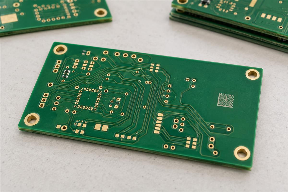
Why does the top surface matter more than the board label?
The surface controls how laser energy is absorbed and what is changed to create contrast. A mark may rely on a color change or controlled material removal. Neither approach is acceptable if it damages a layer that the design still needs.
| Candidate surface | Question before trial | Reason to withhold approval |
|---|---|---|
| Cured solder mask on rigid PCB | What mask formulation, color, thickness and underlying copper are present? | Unintended copper exposure, blistering or loss of protective coverage |
| Exposed laminate | Is direct marking permitted in the designated area? | Charring, fiber exposure or unassessed insulation change |
| Polyimide or flex coverlay | Which film and adhesive construction is actually at the surface? | Distortion, delamination or damage in a bend-critical region |
| Ceramic substrate | What ceramic and surface treatment are specified? | Cracking, chipping or unacceptable alteration near circuitry |
| Exposed metal or plated finish | Is that surface electrically, mechanically or solderably functional? | Damage to a contact, pad, coating or corrosion barrier |
For a masked board, start with the solder-mask construction and process. Two green boards can use different formulations or have different copper below the intended marking area. Successful marking on one is evidence for that sample, not permission to substitute the other.
LPKF’s LaserMicronics service description separates ceramic inscription from solder-resist removal. This distinction matters: deliberately removing a coating during repair is not the same acceptance objective as placing an identification code on an intact finished board. Define what may change before choosing a process.
UV systems are often candidates for heat-sensitive PCB surfaces. KEYENCE’s UV marking explanation describes 355 nm systems and the influence of pulse and repetition settings. However, a “cold marking” description is not proof of zero heat, zero debris or zero damage on your construction. Qualification must inspect the result, not rely on the name of the laser source.
How does a PCB laser marking qualification process work?
Qualify a controlled combination of board, marking area, equipment recipe and acceptance method. The following sequence is a review workflow, not a universal machine operating recipe. Trained personnel should use approved enclosed equipment, interlocks and extraction suitable for the actual materials; unknown coatings should not be trialed casually on an open engraver.
- Identify the surface and construction. Record the board revision, laminate, mask or coverlay designation and the layer beneath the mark. Stop when the coating identity is unknown.
- Define the mark and reserved area. Specify encoded data, symbol type, human-readable text if required, location, orientation and clearance requirements. Avoid silently moving a mark onto pads, traces, bend regions or a removable panel rail.
- Run a controlled sample trial. Let the equipment specialist develop settings on representative scrap or coupons. Record the equipment and recipe revision, focus setup and specimen identity. Do not copy power percentages from another machine.
- Inspect both the symbol and the surface. Check intended data, contrast and geometry, then inspect for local damage. Escalate uncertain depth or layer damage for appropriate engineering examination.
- Repeat the downstream conditions. Include the relevant assembly, cleaning, coating and handling exposures in the validation plan. Read the mark again after those steps, not only immediately after marking.
- Approve the process and change controls. Save the sample identity, inspection evidence, reading conditions and allowed construction range. Require review when a material, mask supplier, marking position or recipe changes.
Consider a controller board whose serial code is readable before assembly but hidden behind a connector afterward. More laser power cannot solve that problem. The marking location needs to be reviewed against the assembled product and the scan station’s view. Similarly, a code placed on a panel rail disappears during depaneling; a panel identifier and an individual-board identifier serve different purposes.
A useful trial compares representative variations deliberately. For example, evaluate the approved mask on locations with and without underlying copper if both occur in the intended design family. Label results by construction. Do not combine those results into one pass statement while losing which sample produced which result.

How do you prove the code is readable and the board is sound?
Use separate checks for data correctness, code quality and board integrity. A scanner decoding one sample does not prove that the mark is robust, and a high-quality symbol does not prove that the laminate beneath it is undamaged.
| Check | Evidence to save | Common false conclusion |
|---|---|---|
| Encoded data and identity | Decoded value matched to the intended serial or lot record | “The scanner beeped, so the content is correct.” |
| Readability in the process | Reader, lighting, distance, orientation and result after relevant downstream steps | “It read once at the bench, so every station will read it.” |
| Formal code quality, where required | Verifier setup and report under the agreed method and acceptance requirement | “An ordinary reader result is a verification grade.” |
| Board integrity | Inspection and relevant electrical or construction evidence for the marked area | “A dark mark means the process is safe.” |
Cognex’s verification documentation explains that verification measures multiple symbol-quality parameters and assigns a grade using defined methods. It also distinguishes direct-part-mark grading from other code applications. Agree the applicable method, revision, illumination and minimum acceptable result with the customer. There is no single grade in this article that automatically applies to every PCB order.
As an illustration, suppose 100 trial boards produce 100 successful decodes before cleaning but only 97 afterward. That is a 97% observed post-cleaning decode rate in this particular trial. It is not evidence of a stable 97% production capability, and it is not an acceptable substitute for a specified verification requirement. Investigate the three failures and the relevant processing conditions before release.
If inspection finds exposed copper where the drawing required intact mask, reject or hold the trial even if every code reads. If the mark passes visual inspection but the depth or insulation effect remains uncertain, choose an appropriate additional evaluation with the board engineer. Do not declare electrical safety from an attractive photograph.
Preserve traceability through rework too. Replacing an unreadable serial mark must not create two boards with one identity or break the link to inspection records. Decide who can authorize re-marking and how the old and new data are reconciled before production starts.
What should you send for a marking feasibility review?
Send the actual surface specification, location and acceptance requirements alongside the fabrication data. “Laser mark this PCB” leaves the supplier to guess the most important constraints.
| Input | Include | Expected review output |
|---|---|---|
| Material identity | Laminate and mask/coverlay designation, color, construction and representative samples | A clearly bounded material trial, not an all-material claim |
| Marking drawing | Coordinates, orientation, reserved area, nearby circuitry and final assembly view | Confirmed location and access through the production route |
| Data definition | Code type, payload, serial allocation and human-readable requirements | Agreed format and identity-control method |
| Acceptance and durability | Reader conditions, required verification method, downstream exposures and inspection needs | Sample report, unresolved issues and release criteria |
Ask the supplier to identify any assumption that could invalidate the trial: another mask formulation, a different mark size, a changed copper pattern beneath the code or a later conformal coating. This converts a general equipment capability statement into a decision tied to your board.
Send PCBtry the board files and marking requirements to discuss a project-specific manufacturing review. Request confirmation of the available marking route and sample-validation scope before approving it. Do not assume a particular laser, wavelength or all-material capability without that confirmation.
PCB laser marking material questions
Can every FR4 PCB be laser marked with the same settings?
No. The exposed surface may be solder mask rather than FR4, and material formulation, thickness and underlying features can differ. A qualified recipe needs a defined construction range.
Does a metal-core PCB require a metal-marking recipe?
Not necessarily. Its circuit side may be coated with solder mask. Identify the surface at the specified marking location rather than choosing by the core name.
Can polyimide flex circuits be marked?
They are a candidate application, but film, coverlay, adhesive construction and bend requirements matter. Validate the exact construction and avoid assuming a successful rigid-board trial transfers to flex.
Can ceramic boards be marked?
Ceramic inscription is an established laser-processing application. The specific ceramic, surface treatment, mark location and permitted alteration still need a trial and inspection.
Is UV marking automatically damage-free?
No. UV may reduce unwanted thermal effects in suitable applications, but the actual recipe and construction determine the outcome. Inspect the marked sample and validate downstream performance.
Does a successful scan prove the mark is acceptable?
No. Check the encoded data and the relevant reading conditions. Formal verification may also be required, and board integrity must be assessed separately.
Should the code be added before or after assembly?
Choose the stage that provides the required traceability and allows safe, accessible marking and reading. Include the remaining processing exposures in validation; neither timing is universally correct.
What changes require another review?
Changes to material, mask or coverlay, marking location, underlying construction, symbol size, recipe or downstream processing can invalidate earlier evidence. Define the review triggers in the approved process record.



0 Comments