




What Does LDI Change in PCB Manufacturing?
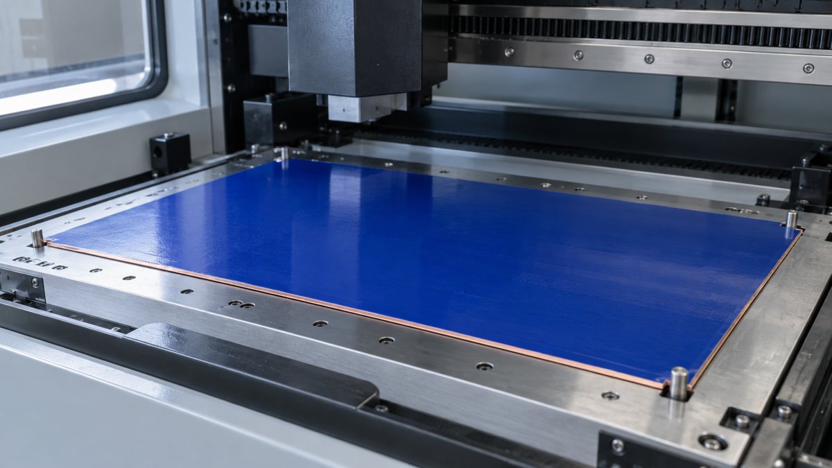
The LDI PCB process uses a computer-controlled laser to expose a circuit pattern in photoresist, a light-sensitive coating on a copper panel. It replaces the physical film phototool used during conventional exposure. Development then reveals the pattern; subsequent etching or plating forms the copper features.
Think of photoresist as a temporary, patterned protective layer. The laser decides where that layer changes chemically. It does not cut the copper traces, drill the vias or test the finished board. Keeping these jobs separate makes both the process and its defects easier to understand.
LDI is useful when image placement, small features or frequent artwork revisions make film handling difficult. However, buying a board described as “LDI manufactured” does not establish its minimum finished line width or reliability. Those depend on the complete qualified fabrication process.
How Does the LDI PCB Process Work?
The practical sequence is approved data → prepared copper → photoresist → target alignment → exposure → development → copper processing and inspection. The route after development differs between inner-layer etching and outer-layer pattern plating.
1. Prepare and approve the manufacturing data
CAM engineering checks the artwork revision, layer order, polarity and critical geometry. The fabricator adds production features and any agreed manufacturing compensation. A mirrored layer or wrong revision can produce a beautifully imaged but unusable board; exposure precision cannot correct incorrect input.
Keep the released Gerber or agreed intelligent manufacturing files together with the drill data, fabrication drawing and stack-up. Ask the fabricator to identify any proposed changes to functional copper before approval. A revision identifier and a comparison against the intended connectivity are more useful than a folder called “final-new.”
2. Prepare the copper and apply the resist
The copper surface must be suitable for adhesion before the light-sensitive coating is applied. For dry film, lamination must produce intimate contact without trapped contamination, wrinkles or bubbles. Surface preparation and lamination settings belong to the qualified material-and-equipment process, not a universal online recipe.
A local adhesion failure can later appear as a missing or narrowed feature even when the exposure file is correct. Inspect the coated panel before imaging and keep suspect panels out of the next stage. Recording the resist product and lot helps distinguish a recurring material issue from a one-panel handling defect.
3. Locate targets and align the digital image
The machine uses registration targets to relate the digital pattern to the actual panel. Depending on the system and process, correction can include position, rotation and scaling. Targets must be recognizable, and the panel must be held within the equipment’s flatness and focus requirements.
A target-recognition failure should trigger a check of the panel, tooling and job setup, not an assumption that the machine will compensate automatically. Registration records are especially useful when an error grows across the panel rather than appearing as a constant offset.
4. Expose the photoresist
The exposure source must match the resist’s spectral sensitivity and qualified dose. For a common negative-working circuit resist, exposed regions become resistant to the developer and remain afterward. A positive-working material behaves differently; do not infer resist chemistry solely from a light or dark image on a screen.
The Riston Laser Series material page lists different products for different wavelengths and fabrication routes. This is why “both are dry film” is not sufficient justification for substitution. Record the approved resist, exposure setup and inspection result together.
5. Develop and inspect the resist pattern
Development removes the soluble parts of the coating. It is not the same operation as copper etching. Inspect whether the required openings are clear, retained resist remains attached, and the pattern matches the approved manufacturing artwork.
If residue remains where copper should be exposed, downstream processing can preserve unwanted copper or interfere with plating. If retained resist is damaged, copper may be attacked or plated where it should not be. Check the development process and resist condition before changing the laser dose: several different causes can produce a similar visual symptom.
6. Complete the appropriate copper route and inspect again
In a typical inner-layer subtractive route, the developed resist protects copper that should remain during etching, then the temporary resist is stripped. In an outer-layer pattern-plating route, resist openings define areas for plating; later stripping and etching steps complete the pattern. Treat these as different process routes, not interchangeable sequences.
Compare the finished copper with its approved manufacturing data. Inspection before lamination is particularly valuable because an internal defect becomes much harder to access afterward. The broader multilayer PCB manufacturing process explains where this handoff fits into the board build.
How Does Digital Registration Handle Panel Movement?
Digital registration measures where reference targets actually sit and adjusts the exposure pattern within the process’s correction capability. It reduces certain alignment errors; it does not make a distorted panel perfect.
Worked example, not a production specification: suppose two targets are nominally 400.00 mm apart, but their measured separation is 399.92 mm. A simple uniform scale factor along that axis would be 399.92 ÷ 400.00 = 0.9998. That represents a 0.02% contraction, or 200 parts per million. Ignoring it leaves an 80 µm mismatch over that span.
This calculation describes only one axis and a uniform change. Rotation, local distortion, target measurement uncertainty and later process movement still matter. The correct acceptance question is therefore “What residual registration error was measured against the agreed references?” rather than “Does the machine have automatic alignment?”
KLA’s Corus platform announcement describes target acquisition, scaling, focus and contamination control as separate equipment features. Its stated specifications apply to that platform; they are not universal tolerances for every finished PCB.
What Sets the Finished Line Width and Spacing?
Finished copper geometry depends on more than the smallest feature an imager can expose. Resist adhesion and thickness, exposure, development, copper thickness and the subsequent etching or plating process all affect the result.
A useful distinction is image capability versus delivered-board capability. A fine line visible in developed resist is an intermediate result. The buyer needs the required conductor and clearance to survive the remaining process within the drawing’s agreed limits.
| Claim or measurement | What it tells you | What still needs confirmation |
|---|---|---|
| Imaging resolution | The exposure system can define a feature under stated conditions | Resist, copper route and finished feature capability |
| Developed resist line width | Exposure and development reproduced the intended resist pattern | Copper geometry after etching or plating |
| Finished conductor width | The inspected copper dimension at the measurement location | Measurement convention, sampling and variation across the panel |
| Registration result | Relative placement against specified targets or features | Reference definition and residual error across the build |
| Electrical test pass | Required connectivity and isolation under the test conditions | Other requirements such as impedance, geometry and reliability |
For a fine-line order, specify the finished conductor and spacing requirements, the layer and copper construction, and where dimensions matter. Let the fabricator propose a qualified route. Do not reduce clearances simply because a machine brochure advertises a smaller laser spot.
Which Defects Should Be Checked After Imaging?
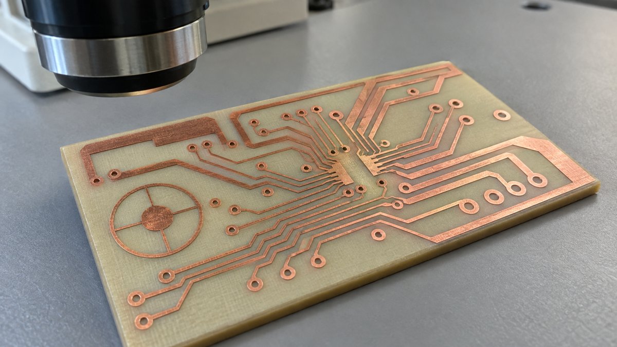
Check the first stage at which a defect appears. Comparing the approved artwork, developed resist and finished copper is more informative than changing exposure settings after every failed board.
| Observed symptom | Possible causes, not a diagnosis | Next check |
|---|---|---|
| Pattern consistently shifted | Wrong target assignment, orientation or registration setup | Verify reference coordinates, job revision and measured target fit |
| Alignment error grows toward the panel edge | Scale mismatch or distortion not represented by the correction model | Compare target residuals across the panel; separate uniform scale from local distortion |
| Resist remains inside an intended opening | Incomplete development, unintended exposure or contamination | Inspect before etching; review developer control, exposure history and material condition |
| Retained resist lifts or has local missing areas | Poor adhesion, particles, damage or an unsuitable process window | Compare coated-panel inspection, lamination records and defect locations |
| Resist pattern looks acceptable but copper is too narrow | Etching variation or incorrect compensation, among other downstream causes | Compare resist and copper measurements from the same feature |
| Repeated defect at the same design coordinate | Artwork/CAM error or a repeatable equipment/process effect | Check the data first, then compare multiple panels and process records |
These checks are an investigation order, not permission to accept a defect. Use the drawing, purchase agreement and applicable acceptance criteria to disposition the board. A photograph without scale, location and process stage is weak evidence for a fine-feature dispute.
When Is LDI Preferable to Film Exposure?
LDI is most useful when removing film handling or improving image-to-panel registration solves a real manufacturing constraint. Conventional film exposure can remain suitable for stable designs comfortably inside a supplier’s qualified process limits.
Compare the full route rather than the exposure step alone. Frequent revisions increase the value of digital data changes. Tight registration and dimensionally sensitive constructions make measured compensation more important. Conversely, a mature board with generous geometry may gain little from a change of exposure method if the existing process already meets its requirements consistently.
Ask both suppliers to quote the same finished requirements, inspection scope, quantity and revision. A promised faster exposure cycle is not a guaranteed shorter order lead time: material availability, downstream operations and factory loading remain relevant. For dense designs, review the project with an HDI PCB manufacturing supplier before committing to marginal geometry.
What Should You Send and Request Before Production?
Send a consistent, revision-controlled manufacturing package and ask for evidence tied to your critical features. “Use LDI” alone is not an adequate fabrication requirement.
- Send: circuit and solder-mask data, drill files, layer order, stack-up, material requirements, copper construction and board outline.
- Identify: critical finished line/space, registration-sensitive pads, fine-pitch mask openings and any controlled-impedance requirements.
- Agree: drawing revision, approval of CAM changes, inspection locations and the acceptance criteria that govern the order.
- Ask: which layers use direct imaging and whether the quoted geometry is qualified for this material, copper and volume.
- Request where warranted: traceable geometry measurements, registration results, relevant inspection findings and electrical-test records.
- Clarify exceptions: any relaxed dimension, missing mask dam or proposed process change should be resolved before release, not discovered on delivery.
A compact supplier question is: “Can you meet the marked finished dimensions on this revision and stack-up, and what inspection record will demonstrate that?” It gives engineering and purchasing the same acceptance target.
LDI PCB Process FAQ
Can direct imaging be used for solder mask?
Yes, compatible photoimageable solder masks can be directly imaged. Mask chemistry, color, coating and curing requirements differ from temporary circuit resist, so the qualified solder-mask process must be confirmed separately.
Can any dry film be used in an LDI machine?
No. Wavelength response, required exposure energy, thickness and compatibility with the intended etching or plating route must match. A substitution needs process qualification rather than an assumption based on film appearance.
Is LDI useful for prototypes?
It can be, especially where artwork changes frequently or registration is difficult. Prototype quantity alone does not establish a cost or lead-time advantage; compare the actual supplier route and quotation.
Is LDI the same as laser drilling?
No. LDI exposes a light-sensitive coating to define a pattern. Laser drilling removes material to create holes; the machines, process controls and acceptance requirements are different.
Are Gerber files enough to order an LDI PCB?
Gerbers describe artwork, but the fabricator also needs the relevant drilling, stack-up, material and fabrication requirements. Missing instructions about finished copper or critical tolerances cannot be recovered simply by using a precise imager.
Does AOI replace electrical testing?
No. Optical inspection checks visible pattern features, while electrical testing checks connectivity and isolation under specified conditions. They provide different evidence and should follow the inspection plan for the board.
Does LDI guarantee controlled impedance?
No. Trace geometry is only part of the impedance problem; dielectric construction and other stack-up factors also matter. Specify the required impedance and agreed verification method separately.
Is there one recommended exposure-energy setting?
No. Use the current material guidance and the qualified machine/process combination. A dose copied from another film, thickness or imager can produce an unacceptable pattern even when the numerical setting appears reasonable.
Preparing a fine-line PCB for manufacture? Send the approved artwork, drill files, stack-up, copper requirements and marked critical dimensions through PCBtry’s contact page. Request a project-specific manufacturability review and confirmation of the inspection evidence before releasing the order.



0 Comments