




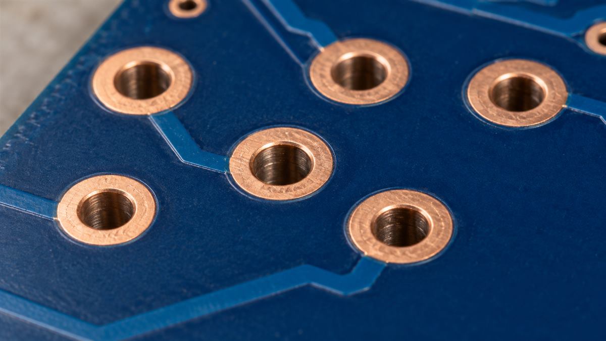
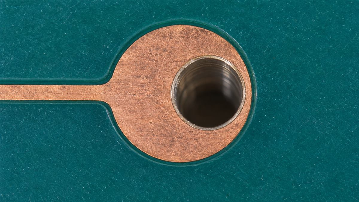
A PCB annular ring is the copper remaining around a hole in a copper pad. For a centered circular hole, its width is (pad diameter – hole diameter) / 2. The important qualification is which hole diameter you use: a finished opening and a manufacturing drill are not necessarily the same size. A nominal ring that looks sufficient in CAD can become too narrow after drilling and layer-registration errors.
Before accepting a pad size, answer three questions: Which hole size does the rule use? How much copper must remain at the narrowest point? Has the fabricator allowed for its manufacturing process? Those answers are more useful than copying an unexplained minimum from a capability table.
How Do You Calculate PCB Annular Ring Width?
Subtract the hole diameter from the copper-pad diameter, then divide by two. You divide by two because the diameter difference includes copper on both sides of the hole. The result is a width measured across the board surface, not the copper thickness or the thickness of plating inside the hole.
Picture a circular copper pad with a hole through its center. The pad is the full copper land; the ring is the portion left around the opening. A plated hole has conductive metal along its wall. At a connected layer, the land joins that wall to the circuit. A component hole can also provide a solderable connection for a lead. Solder mask is a separate coating and does not add copper to this ring.
- Identify the copper pad. Use its copper dimensions, not its solder-mask opening. For this first calculation, use a circular pad and a circular hole.
- Identify the hole basis. Record whether the value is a drill diameter, a finished-hole diameter, or a CAD field whose manufacturing meaning needs confirmation.
- Use one unit throughout. One mil is 0.001 inch, or 0.0254 mm. It is not one millimeter.
- Calculate and label the result. Write the hole basis beside the calculated width so another engineer can reproduce it.
Example: a 0.60 mm circular pad surrounding a centered 0.30 mm hole gives (0.60 – 0.30) / 2 = 0.15 mm, approximately 5.91 mil. This is a geometric example, not a recommended production rule. If the hole moves off-center, the two sides no longer have the same width.
The reverse calculation is useful when selecting a pad: pad diameter = hole diameter + 2 x required nominal ring width. It does not, by itself, include manufacturing allowances. Add those only after establishing what the fabricator’s design rule already includes.
Which Hole Diameter Should You Use?
Use the diameter specified by the particular design or inspection rule. For manufacturing checks, that is often the drill diameter before plating. For finished external-ring measurement, the finished opening is relevant. For internal-layer ring evaluation, the drilled boundary matters; copper plated inward later does not restore inner-layer copper already removed by drilling.
| Question being answered | Relevant basis | What to confirm |
|---|---|---|
| Will a component lead fit? | Finished hole and its tolerance | Lead dimensions, insertion clearance and final finish |
| Can the fabricator drill the pad without losing required copper? | Actual manufacturing drill or agreed CAM rule | Drill compensation and registration allowance |
| How much external ring remains on the finished board? | Finished plated opening and final outer land | Shortest measured distance under the applicable acceptance requirement |
| How much internal land survives drilling? | Drilled boundary and internal land | Layer-specific registration and the required inspection method |
Summit Interconnect’s annular-ring explanation distinguishes external finished-hole measurement from internal drill-based measurement. That distinction is why two tables can use the same phrase, “minimum annular ring,” while describing different checks.
Second example: keep the 0.60 mm pad and suppose an agreed process uses a 0.40 mm drill to obtain a nominal 0.30 mm finished hole. The centered drill-based ring is (0.60 – 0.40) / 2 = 0.10 mm. The centered finished-opening calculation is 0.15 mm. Both calculations can be arithmetically correct; they answer different questions.
The 0.10 mm diameter difference in this example is an assumption, not a universal plating allowance. Eurocircuits describes its own drill compensation when explaining this effect. Other processes, finishes and hole requirements can use different compensation. Do not automatically add a fixed amount to every drill file.
Also ask what the CAD tool’s hole-size field means in your delivery workflow. Many orders specify finished plated holes and let CAM select the tool; other instructions explicitly identify drill sizes. State the convention in the fabrication notes. For the wider manufacturing context, see how PCB vias are drilled and plated.
How Much Ring Remains After Manufacturing Tolerances?
The narrowest remaining ring is smaller than the centered value when the hole and pad are misaligned. For circular boundaries, a simple geometric check is minimum remaining width = (actual pad diameter – actual hole diameter) / 2 – center offset. Use consistent boundaries: do not combine an internal drilled-hole requirement with an external finished-opening measurement.
Consider a deliberately simplified internal-layer example. All values below are hypothetical limits agreed for that example, not measured PCBtry capability or IPC acceptance values.
| Input or result | Value | Meaning |
|---|---|---|
| Nominal copper-pad diameter | 0.60 mm | Layout value |
| Smallest actual pad diameter | 0.58 mm | Assumed size allowance after processing |
| Largest drilled-hole diameter | 0.41 mm | Assumed drill-size upper bound |
| Maximum relative center offset | 0.04 mm | Assumed combined radial registration bound |
| Narrowest remaining ring | (0.58 – 0.41) / 2 – 0.04 = 0.045 mm | 45 micrometers under these assumptions |
| Example agreed minimum | 0.05 mm | The calculated 0.045 mm would not meet this particular requirement |
To reach the example’s 0.05 mm minimum, the actual pad would need to be at least 0.41 + 2 x (0.05 + 0.04) = 0.59 mm. If the assumed pad-diameter reduction remains 0.02 mm, that suggests a nominal pad of at least 0.61 mm under this model. Designing exactly at the calculated limit leaves no extra margin; the fabricator must confirm the assumptions and suitable production target.
This model keeps size error separate from position error. A hole-diameter tolerance of +/-0.02 mm is not automatically a center-position tolerance of +/-0.02 mm. Similarly, an X/Y location tolerance is not automatically the same as a radial offset bound. Ask how the stated tolerance is defined before putting it into an equation.
Do not count an allowance twice. If the manufacturer’s minimum CAD ring already incorporates its drill compensation and registration budget, adding those same allowances again may produce an unnecessarily large pad. Conversely, a finished-board acceptance minimum usually is not enough information to choose a CAD pad directly.
A root-sum-square statistical estimate is also not a guaranteed worst-case bound. Combining independent statistical errors can be useful in process analysis, but only with justified distributions and acceptance risk. For a design release, obtain the fabricator’s approved design rules or an explicitly agreed tolerance model.
What Minimum Annular Ring Should You Specify?
Specify both the design requirement and the finished-board acceptance requirement, with their measurement basis. There is no defensible single minimum that covers all mechanically drilled holes, microvias, layers, copper weights and product requirements.
Three different numbers often get confused:
- CAD minimum: the ring your layout must provide using an agreed hole convention.
- Fabrication capability: what the selected process can reliably manufacture for your stackup and features.
- Acceptance minimum: what the delivered board must meet under its applicable specification.
IPC design guidance and finished-board requirements serve different purposes. State the applicable standard, revision, product class and any relevant addendum or agreed exception. Do not assume a table labeled Class 2 or Class 3 is complete without its layer type, hole type, measurement definition and acceptance conditions. This article deliberately does not reproduce an unverified universal IPC limits table.
Use these questions before fixing the padstack:
- Is this a component hole, through via, blind via, buried via or microvia?
- Which connected layers need lands, and what diameter is required on each?
- Does the published minimum use the finished hole or manufacturing drill?
- Which compensation and positional allowances are already included?
- What remaining ring, breakout restrictions and conductor-junction conditions apply?
- How will compliance be inspected and documented for this order?
A visible ring need not be perfectly concentric to meet an agreed requirement. Equally, a positive but very narrow ring is not automatically acceptable. Tangency means the hole boundary touches the land boundary at a point; breakout means it extends beyond that boundary. These describe geometry. Acceptance depends on the full specification, not on the label alone.
How Do You Fix an Annular-Ring DFM Failure?
First establish whether the finding is a real shortage of copper or a mismatch in hole-size interpretation. Then change the feature with the least unintended impact. Do not dismiss a fabrication warning merely because CAD DRC reports no error: the two checks may use different hole compensation or pad definitions.
| Possible change | When it helps | Check before release |
|---|---|---|
| Increase the affected pad diameter | More copper is needed and space exists | Trace clearance, nearby plane features, solder-mask geometry and sensitive signal behavior |
| Reduce a via hole with fabricator approval | The via does not require the original finished opening | Plating feasibility, aspect ratio, electrical/thermal requirements and test access |
| Change routing or via placement | Dense routing prevents a larger land | Connectivity, escape routing, return paths and spacing on every affected layer |
| Review the via structure or fabrication process | The current structure cannot meet the required density and margin | Stackup, layer pairs, lamination sequence, qualification scope and cost |
| Add a teardrop at the trace-to-pad junction | Local copper reinforcement is useful | Clearance and junction geometry; it does not create an adequate ring everywhere |
For a through-hole component, do not shrink the finished hole merely to make the ring check pass. The lead still has to fit, with the required manufacturing and assembly tolerances. Increasing the pad, relocating the feature or revising the footprint may be the appropriate solution instead.
Teardrops are copper extensions added in the design or an approved CAM change before manufacture. They can protect a trace-to-land connection against some registration variation. They do not restore copper already removed on a defective finished board, repair a short circuit, or waive the specified ring requirement. Ask the fabricator before allowing automatic changes to electrically sensitive geometry.
Changing to a blind or buried structure is not just changing a drill symbol. Review the affected via layer pairs and manufacturing sequence. For a layout that needs rework around crowded pads, PCB design support can be a useful next step; provide the actual padstack and DFM finding rather than only a screenshot.
How Do You Verify Rings and Release the Board?
Verify the exported manufacturing data first, then agree how the fabricated features will be checked. DRC, CAM review, visual inspection, sectioning and electrical tests provide different evidence. No single “pass” establishes every aspect of ring geometry and long-term reliability.
- CAD DRC: checks the geometry and rules actually configured. An incorrect hole convention can still produce a clean report.
- CAM/DFM review: checks delivered artwork and drill data against the intended manufacturing process. Request the affected layer, pad size, interpreted hole size and required correction.
- External optical inspection: can assess accessible outer copper and hole placement. Mask coverage or a poor image can obscure the measurement.
- Internal inspection: requires an agreed method appropriate to the feature. A microsection examines a selected plane, not automatically the smallest ring around every hole in the lot. Ask how samples and section orientation are selected.
- Electrical testing: identifies continuity and isolation defects within the test coverage. Passing it does not prove every ring dimension or predict lifetime under thermal cycling.
Before releasing the board, use this handoff checklist:
- One consistent revision: copper artwork, drill files, layer order and fabrication drawing belong to the same release.
- Explicit hole definitions: plated versus non-plated, finished versus tool size, tolerances, slots and blind/buried spans are identified.
- Layer-specific padstack: pad sizes and connected layers are supplied; a top-view screenshot alone is not enough.
- Agreed requirements: material, copper, finish, applicable standard/revision/class, ring acceptance and any approved exceptions are documented.
- Closed DFM findings: revised files are checked again and approved changes are traceable. Do not accept an unexplained “we will fix it.”
- Inspection evidence: agree which reports or sample results accompany the order and how a nonconforming finding is handled.
A useful request is: “For the marked holes, please confirm the drill-size interpretation, minimum land required on each connected layer, allowances included in your rule, and the finished-ring acceptance and verification method.” This makes the review specific enough for an engineer to answer.
PCB Annular Ring FAQ
Does a non-plated mounting hole need an annular ring?
Not necessarily. A non-plated mechanical hole may deliberately have no copper pad and require a copper keepout instead. If a mounting feature needs an electrical connection, such as chassis grounding, define that separately. Do not let the presence of a visible copper circle decide whether a hole should be plated; state the intended construction in the manufacturing data.
Can the circular formula be used for an oblong pad or plated slot?
Not as a complete check. A slot or irregular land has different remaining distances at its sides, ends and trace junctions. Evaluate the shortest relevant distances using the actual shapes and agreed manufacturing allowances. Ask the fabricator for its slot and land requirements; an equivalent circular diameter can hide the narrowest location.
Can microvias use the same rule as mechanically drilled through vias?
Do not assume so. Laser-formed microvias have different geometry, capture and target lands, alignment controls and process requirements. A through-via minimum copied into a microvia padstack may be unnecessarily large or still miss an important constraint. Use the fabricator-approved microvia structure and evaluate its reliability requirements separately from simple ring-width arithmetic.
Does tenting a via change its copper annular ring?
Tenting changes the solder-mask treatment, not the underlying copper land or drilled geometry. It can hide the opening from an ordinary surface view, but it does not add missing copper. Keep solder-mask rules separate from copper-ring rules, and clarify how covered features will be inspected when visible access is needed.
Does a wider ring automatically give a via a higher current rating?
No. Current performance also depends on barrel copper, hole geometry, board thickness, heat dissipation, connections and allowable temperature rise. A wider land may improve a local connection without making the entire via adequate for the required current. Use an appropriate electrical and thermal assessment rather than assigning a current rating from ring width alone.
Must an unconnected internal layer retain a pad around every via?
Not universally. Nonfunctional-pad removal is a separate design and fabrication decision; it must not remove a required connected land or violate spacing and reliability requirements. State the permitted treatment in the fabrication notes and review the resulting padstack. A removed nonfunctional pad is not the same defect as an intended connected land lost to drill breakout.
Are annular rings relevant to a single-sided board?
Yes, a copper land around a component hole can be important for soldering and mechanical attachment even without an interlayer plated connection. However, do not transfer multilayer plated-hole acceptance rules automatically. Identify whether the hole is plated and what assembly and product requirements apply to the particular single-sided construction.
Why does a supplier ask for a larger ring than a published minimum?
The quoted minimum may describe a finished feature, a different manufacturing option, or a simpler stackup. Your design may need a larger starting land to allow for registration and process variation. Request the basis and included allowances. Compare like-for-like definitions before concluding that either the supplier or the design software is wrong.
Need an annular-ring check before fabrication? Send PCBtry the current Gerber or agreed manufacturing package, drill table, stackup, padstack details and the marked DFM findings. Include your hole-size convention and applicable acceptance requirements. Request a design and manufacturing review, or email sales@pcbtry.com, and ask for the required pad or drill changes in writing before approving production.



0 Comments