
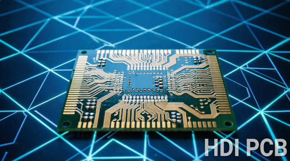
An HDI PCB, or high density interconnect printed circuit board, is designed with finer traces, smaller vias, higher wiring density, and advanced layer structures to support compact, high-performance electronics. It is widely used when a conventional PCB cannot provide enough routing space, signal performance, or miniaturization for modern products.
For engineers and buyers, HDI PCB technology is not only about making a board smaller. It affects signal integrity, thermal behavior, component placement, assembly yield, reliability testing, production cost, and long-term supply stability. A well-designed HDI PCB can reduce product size, improve electrical performance, and support complex chips such as BGAs, processors, RF modules, sensors, and high-speed communication devices.
What Is an HDI PCB?
An HDI PCB is a printed circuit board that uses high-density routing features such as microvias, blind vias, buried vias, fine lines, fine spacing, and compact layer build-ups. Compared with a standard multilayer PCB, an HDI PCB provides more interconnection points within a smaller board area.
In practical manufacturing, HDI PCB designs often use laser-drilled microvias, sequential lamination, via-in-pad structures, and thin dielectric materials. These features allow engineers to fan out fine-pitch components and route dense circuits without increasing the board size. This makes HDI PCB fabrication essential for smartphones, wearables, automotive electronics, medical devices, communication systems, AI hardware, and industrial control modules.
The core value of HDI PCB technology is routing efficiency. When component pitch becomes smaller and signal speed becomes higher, ordinary through-hole vias can consume too much space and introduce unwanted electrical effects. HDI structures solve this problem by shortening interconnect paths and improving layout flexibility.
Why HDI PCB Matters in Modern Electronics
HDI PCB matters because modern electronic products require smaller size, higher speed, lower weight, and more functions on the same or smaller board area. Without HDI PCB technology, many compact devices would need larger boards, more layers, or compromised routing quality.
For engineering teams, HDI PCB design helps solve three common challenges: dense component fan-out, high-speed signal routing, and miniaturized product structure. For purchasing teams, it helps reduce total product size and may lower system-level cost, even if the bare PCB price is higher than a standard board.
HDI PCB is especially valuable when a design includes fine-pitch BGA packages, high-pin-count processors, RF circuits, camera modules, memory chips, or mixed analog-digital layouts. In these cases, routing density and signal path length become critical. A well-planned HDI stack-up can improve manufacturability and reduce the risk of repeated redesigns.
How HDI PCB Technology Works
HDI PCB technology works by replacing space-consuming through-hole routing with smaller and more efficient interconnect structures. The most important feature is the microvia, usually produced by laser drilling and used to connect adjacent or selected internal layers.
A typical HDI PCB may use blind vias from the outer layer to an inner layer, buried vias between internal layers, or stacked and staggered microvias for advanced routing. Sequential lamination is often required because some vias must be formed and plated before additional layers are laminated on top.
In manufacturing, HDI PCB production requires tighter process control than standard PCB fabrication. Laser drilling accuracy, copper plating uniformity, resin filling, lamination pressure, registration control, surface finish quality, and electrical testing all influence the final yield. This is why early design review is important before releasing HDI PCB files for production.
Main HDI PCB Structures and Types
HDI PCB structures are usually selected according to routing density, component pitch, layer count, reliability requirements, and production cost. A more advanced structure can solve routing problems, but it also increases manufacturing complexity.
| HDI PCB Type | Typical Use | Relative Cost | Key Limitation |
|---|---|---|---|
| 1+N+1 HDI PCB | Consumer electronics, compact control boards, moderate BGA routing | Medium | Limited routing density compared with advanced HDI structures |
| 2+N+2 HDI PCB | Smart devices, communication modules, medical electronics | Medium to high | Requires more sequential lamination and tighter process control |
| Any-layer HDI PCB | High-end mobile devices, AI modules, advanced compact electronics | High | Complex fabrication, higher yield risk, stricter supplier capability needed |
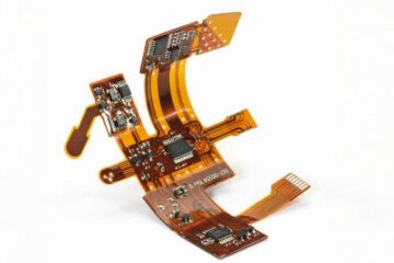
| Rigid-flex HDI PCB | Wearables, cameras, medical devices, foldable electronic assemblies | High | Material selection, bending reliability, and assembly control are critical |
| High-frequency HDI PCB | RF front-end, 5G modules, radar, satellite communication | High | Requires low-loss materials and precise impedance control |
For most projects, the best HDI PCB structure is not the most advanced one. It is the structure that provides enough routing space, stable yield, acceptable cost, and reliable long-term production. Over-designing the stack-up can increase cost without improving product performance.
HDI PCB Materials and Surface Finishes
HDI PCB materials must support fine-line manufacturing, stable lamination, reliable microvia plating, and the electrical requirements of the final application. FR-4 is still widely used, but high-speed, high-frequency, automotive, and medical designs may require more advanced materials.
Common HDI PCB material choices include standard FR-4, high-Tg FR-4, low-loss laminates, halogen-free materials, flexible polyimide, and specialty high-frequency materials. Material selection should consider glass transition temperature, coefficient of thermal expansion, dielectric constant, dissipation factor, copper foil type, and thermal reliability.
Surface finish also matters. ENIG is commonly used for fine-pitch components because it provides good solderability and flatness. OSP may be suitable for cost-sensitive applications with controlled storage and assembly conditions. Immersion silver, immersion tin, and other finishes may be selected according to soldering process, shelf life, bonding requirements, and product environment.
| Material or Finish | Suitable Application | Main Advantage | Design Note |
|---|---|---|---|
| High-Tg FR-4 | Industrial control, automotive electronics, multilayer HDI | Better thermal stability than standard FR-4 | Useful when reflow cycles and operating temperature are demanding |
| Low-loss laminate | High-speed data, RF, communication equipment | Lower signal loss at higher frequencies | Impedance planning must be confirmed before fabrication |
| Polyimide | Flexible and rigid-flex HDI PCB | Good flexibility and thermal performance | Bend radius and copper fatigue must be reviewed carefully |
| ENIG | BGA, fine-pitch SMT, high-reliability assembly | Flat surface and good solderability | Process control is important for long-term reliability |
| OSP | Cost-sensitive SMT products | Lower cost and simple process | Storage time and handling conditions must be controlled |
Key HDI PCB Design Rules Engineers Should Check
HDI PCB design requires early coordination between the layout engineer, PCB manufacturer, and assembly team. Small design choices can strongly affect fabrication yield and assembly reliability.
The first rule is to confirm the manufacturer’s actual capability before finalizing trace width, spacing, laser via size, annular ring, dielectric thickness, via stack structure, and copper thickness. A design that looks correct in CAD software may still be difficult or expensive to build if it sits too close to the factory’s process limit.
Engineers should also pay close attention to BGA fan-out strategy. Fine-pitch BGAs often require via-in-pad, filled vias, or microvias to route signals cleanly. If the via structure is not planned correctly, solder voiding, pad flatness issues, escape routing failure, or impedance discontinuity may appear during prototype assembly.
Another common design issue is insufficient test access. HDI PCB layouts are dense, but test points are still necessary for debugging, production inspection, and failure analysis. If space is limited, test pads should be prioritized for power rails, programming interfaces, reset signals, communication buses, and critical high-risk nets.
HDI PCB Manufacturing Process
HDI PCB manufacturing is more complex than standard multilayer PCB production because it often includes laser drilling, sequential lamination, fine-line imaging, microvia plating, and strict registration control.
A typical HDI PCB process starts with engineering file review and stack-up confirmation. The manufacturer checks Gerber data, drill files, impedance notes, material requirements, controlled depth structures, copper thickness, solder mask clearance, surface finish, and special tolerances. After CAM preparation, inner layers are imaged and etched, then laminated according to the required build-up structure.
Laser drilling is used to create microvias. These vias are then cleaned, metallized, and plated to build reliable electrical connections. For via-in-pad designs, via filling and planarization may be required to create a flat soldering surface. After the final lamination and outer-layer processing, the board goes through solder mask, surface finish, routing, inspection, and electrical testing.
The most difficult part is consistency. HDI PCB production depends on stable copper plating, accurate layer registration, controlled lamination movement, and clean microvia formation. A supplier experienced in HDI PCB fabrication should review risk points before production instead of simply accepting files without questions.
HDI PCB Testing and Quality Standards
HDI PCB testing verifies whether the board can meet electrical, mechanical, thermal, and reliability requirements before assembly or shipment. For high-density boards, testing is not optional; it is a core part of risk control.
Common quality checks include automated optical inspection, electrical testing, microsection analysis, solder mask inspection, impedance testing, dimensional inspection, and surface finish inspection. For assembled HDI PCB projects, AOI, X-ray inspection, in-circuit testing, and functional testing may also be used.
Recognized standards such as IPC specifications, UL requirements, RoHS compliance, ISO 9001 quality management, ISO 13485 medical manufacturing controls, and IATF 16949 automotive production requirements can help define consistent quality expectations. Thindry supports certified manufacturing systems including ISO 9001, ISO 13485, IATF 16949, UL certified PCBs, and RoHS compliant production for suitable project requirements.
For high-reliability HDI PCB projects, microsection analysis is especially valuable. It can reveal microvia plating quality, copper thickness, dielectric condition, lamination bonding, resin filling quality, and possible cracks that may not be visible during normal inspection.
Advantages and Limitations of HDI PCB
HDI PCB offers strong advantages in compact, high-performance electronics, but it also introduces higher design and manufacturing requirements. Understanding both sides helps avoid unnecessary cost and production risk.
| Factor | HDI PCB Advantage | Possible Limitation | Practical Recommendation |
|---|---|---|---|
| Board size | Supports smaller and lighter products | Dense layout may reduce test access | Reserve critical test points early in layout |
| Routing density | Improves BGA fan-out and signal routing | Advanced structures increase fabrication cost | Choose only the HDI level the design truly needs |
| Signal performance | Shorter interconnects can reduce parasitic effects | Poor stack-up planning can still cause impedance issues | Confirm impedance and return path before fabrication |
| Assembly | Works well with fine-pitch SMT packages | Via-in-pad requires excellent filling and flatness | Use controlled via filling for BGA pads |
| Reliability | Can support demanding compact products | Microvia fatigue or plating defects may occur if process is weak | Use qualified suppliers and proper reliability testing |
The most common mistake is choosing HDI PCB only because a product needs to look advanced. HDI should be selected when it solves a real routing, size, performance, or assembly problem. If a standard multilayer PCB can meet the design requirement reliably, it may remain the better choice.
HDI PCB Applications Across Major Industries
HDI PCB is used in industries where space, performance, reliability, and signal quality are important. The specific structure and material choice vary by application.
In consumer electronics, HDI PCB is common in smart TVs, wearables, earbuds, gaming devices, digital cameras, smart home products, and compact control boards. These products often require thin boards, high-density routing, flexible interconnects, and cost-efficient production.
In automotive electronics, HDI PCB supports battery management systems, vehicle control units, motor controllers, onboard chargers, ADAS modules, cameras, radar systems, cockpit electronics, lighting controls, and seat control modules. Automotive applications often require high reliability, wide temperature performance, vibration resistance, thermal stability, and long service life.
In communication equipment, HDI PCB is used in 5G and 6G infrastructure, optical modules, switches, routers, server backplanes, satellite communication systems, and RF front-end modules. These boards often require controlled impedance, low-loss materials, precise registration, and advanced multilayer construction.
In AI servers and data centers, HDI PCB technology helps support GPU cards, FPGA acceleration boards, storage devices, and high-speed switching systems. These applications may require ultra-high layer counts, strict impedance control, low insertion loss, excellent flatness, and strong thermal management.
Industrial, medical, aerospace, renewable energy, LED lighting, IoT, AR/VR, and semiconductor packaging applications also use HDI PCB structures when miniaturization, reliability, electrical stability, and advanced interconnection are required.
Real Engineering Cases and Practical Lessons
HDI PCB problems often appear during prototype debugging or early mass production. Many failures are not caused by a single process defect, but by design decisions that did not match real manufacturing limits.
One common case is fine-pitch BGA escape routing. A design may pass electrical rule checks but fail during production because the selected via size, pad design, or via-in-pad filling requirement was not confirmed with the factory. The result can be poor solder joint quality or assembly yield loss. The practical lesson is simple: confirm the HDI stack-up and via structure before completing the final BGA layout.
Another frequent issue is impedance mismatch on compact high-speed boards. When trace geometry, dielectric thickness, copper roughness, and reference plane continuity are not coordinated, the finished board may not meet the expected signal performance. The solution is to define controlled impedance requirements clearly and let the manufacturer calculate the stack-up before fabrication.
A third case involves rigid-flex HDI PCB products used in wearable or camera modules. If the bending area includes unsuitable copper layout, sharp corners, or incorrect stiffener placement, fatigue failure may occur after repeated movement. The best practice is to separate dynamic bending areas from dense interconnection zones and review bend radius early.
Common HDI PCB Failure Modes and Prevention
HDI PCB failure analysis should focus on microvia reliability, lamination quality, soldering behavior, material stability, and assembly stress. Because HDI boards are dense, small defects can create serious field problems.
Microvia failure is one of the most important risks. Poor laser drilling, weak copper plating, contamination, or thermal cycling stress may cause intermittent opens or complete electrical failure. Microsection inspection and controlled plating processes help reduce this risk.
Via-in-pad solder defects are also common when via filling or planarization is not properly controlled. If the pad is not flat or the via absorbs solder, BGA solder joints may become weak or inconsistent. Filled and capped vias are usually recommended for fine-pitch BGA pads.
Delamination may occur when materials, lamination cycles, moisture control, or thermal stress are not properly managed. This risk increases in multilayer HDI PCB designs with multiple lamination cycles. Baking control, suitable material selection, and proper process qualification are essential.
Other common issues include solder mask registration errors, insufficient annular ring, copper cracking in flex zones, poor impedance control, CAF risk, warpage, and assembly yield loss caused by overly dense placement. Most of these problems can be reduced through early DFM review.
How to Choose the Right HDI PCB Solution
The right HDI PCB solution should match the product’s routing density, performance target, reliability requirement, assembly process, and budget. The best starting point is not the layer count, but the problem the board must solve.
If the design uses fine-pitch BGAs, begin with fan-out analysis. If the product requires high-speed data transmission, begin with stack-up and impedance planning. If the product must fit a tight mechanical space, begin with board thickness, connector position, bending requirement, and assembly clearance. If the product will be used in harsh environments, begin with material reliability and testing requirements.
For prototype projects, a slightly more conservative design can reduce revision risk. For mass production, cost optimization should focus on reducing unnecessary lamination cycles, avoiding over-tight tolerances, standardizing material choices, improving panel utilization, and confirming component availability before assembly.
A reliable HDI PCB manufacturer should be able to suggest manufacturable alternatives, not only quote the lowest price. For example, changing from stacked microvias to staggered microvias, adjusting BGA escape routing, or modifying the stack-up may improve yield and reduce cost without hurting performance.
HDI PCB Cost Factors and Procurement Advice
HDI PCB cost is affected by layer count, build-up structure, microvia complexity, material type, line width and spacing, copper thickness, via filling, surface finish, impedance control, testing requirements, panel utilization, quantity, and delivery speed.
Buyers should avoid comparing HDI PCB quotes only by unit price. A cheaper quotation may exclude controlled impedance, electrical testing, via filling, special material, reliability inspection, or assembly-related requirements. These missing items can create higher costs later through redesign, failed prototypes, or poor production yield.
For overseas buyers sourcing from a China-based manufacturer, the practical advantages often include integrated PCB fabrication, component sourcing, PCBA assembly, engineering review, scalable production capacity, and flexible customization. The key is to keep communication clear and technical: provide complete Gerber files, stack-up notes, BOM, pick-and-place files, assembly drawings, impedance requirements, inspection expectations, and target application details.
Thindry focuses on PCB design, PCB prototype, PCB manufacturing, and PCB assembly services. With automated production, engineering support, quality systems, and one-stop electronics manufacturing capability, the team can support HDI PCB projects from early sample development to batch production and global delivery.
HDI PCB Supplier Selection Checklist
An HDI PCB supplier should be selected based on engineering capability, process control, quality systems, communication efficiency, and production scalability. HDI projects are too sensitive to be managed only as commodity board orders.
| Checklist Item | Why It Matters | What to Confirm Before Ordering |
|---|---|---|
| HDI process capability | Ensures the supplier can build your microvia and fine-line structure | Minimum line width, spacing, laser via size, via filling, and layer build-up options |
| Engineering review | Prevents avoidable design and manufacturing errors | DFM feedback, stack-up review, impedance support, BGA fan-out review |
| Quality certification | Supports consistent production and industry compliance | ISO 9001, ISO 13485, IATF 16949, UL, RoHS where applicable |
| Testing capability | Reduces risk before assembly and shipment | Electrical test, AOI, microsection, impedance testing, X-ray for assembly |
| PCBA support | Improves prototype debugging and production coordination | SMT, THT, mixed assembly, BOM optimization, MES tracking, functional testing |
| Global delivery experience | Helps overseas buyers manage lead time and documentation | Packing method, export documents, delivery terms, and communication workflow |
Before placing an order, prepare a complete technical package. At minimum, include Gerber files, drill files, stack-up requirements, material preference, copper thickness, surface finish, impedance targets, solder mask color, board thickness, tolerance notes, BOM, pick-and-place files, assembly drawings, and functional test requirements if PCBA is needed.
FAQ About HDI PCB
What does HDI PCB mean?
HDI PCB means high density interconnect printed circuit board. It uses finer traces, smaller spacing, microvias, blind vias, buried vias, and compact layer structures to create more routing capacity in less space. It is commonly used when a standard PCB cannot support dense components or compact product design.
When should I use an HDI PCB instead of a standard PCB?
You should consider an HDI PCB when your design includes fine-pitch BGAs, limited board area, high pin-count components, high-speed signals, RF circuits, or strict miniaturization requirements. If a standard multilayer PCB can meet routing and reliability needs, HDI may not be necessary.
Is HDI PCB more expensive?
Yes, an HDI PCB is usually more expensive than a standard PCB because it may require laser drilling, sequential lamination, microvia plating, via filling, tighter registration, and more inspection. However, it can reduce overall product size and may lower system-level cost in compact electronics.
What is a microvia in HDI PCB?
A microvia is a small via, typically laser-drilled, used to connect layers in an HDI PCB. It allows dense routing and helps engineers escape signals from fine-pitch components. Microvia quality is critical because poor plating or thermal fatigue can cause reliability problems.
What is the difference between blind vias and buried vias?
A blind via connects an outer layer to one or more inner layers without passing through the entire board. A buried via connects only internal layers and is not visible from the outside. Both are used in HDI PCB designs to save routing space and improve layout density.
Can HDI PCB support high-speed signals?
Yes, HDI PCB can support high-speed signals when the stack-up, impedance, reference planes, material selection, and routing rules are properly designed. Shorter interconnects can help reduce parasitic effects, but poor impedance planning can still cause signal integrity problems.
Which surface finish is best for HDI PCB?
ENIG is commonly selected for HDI PCB designs with BGA and fine-pitch SMT components because it provides a flat surface and good solderability. OSP can be used for cost-sensitive projects, but storage and handling conditions must be controlled carefully.
What files are needed for an HDI PCB quote?
For an accurate HDI PCB quote, provide Gerber files, drill files, stack-up information, material requirements, copper thickness, surface finish, board thickness, impedance notes, tolerance requirements, and quantity. For PCBA, also include BOM, pick-and-place files, and assembly drawings.
Why do HDI PCB prototypes fail during assembly?
Common reasons include incorrect footprints, poor via-in-pad design, insufficient solder mask clearance, unfilled vias under BGA pads, warpage, poor surface finish control, or missing DFM review. Many assembly failures can be prevented by confirming fabrication and assembly requirements before production.
Can HDI PCB be used in automotive electronics?
Yes, HDI PCB is used in automotive electronics such as BMS, ADAS modules, radar, cameras, cockpit systems, and control units. Automotive projects require strong reliability control, suitable materials, thermal stability, vibration resistance, and production systems aligned with automotive quality expectations.
How long does HDI PCB manufacturing take?
Lead time depends on layer count, build-up structure, material availability, via filling, impedance testing, quantity, and assembly requirements. Simple HDI prototypes may move faster, while advanced multilayer or rigid-flex HDI projects need more engineering review and process time.
How can I reduce HDI PCB cost without hurting quality?
You can reduce cost by avoiding unnecessary lamination cycles, using manufacturable line width and spacing, improving panel utilization, selecting standard materials where suitable, simplifying via structures, and confirming component availability early. Cost reduction should never remove essential testing or reliability controls.
What makes a good HDI PCB manufacturer?
A good HDI PCB manufacturer has stable microvia capability, strong engineering review, reliable lamination and plating control, quality certifications, testing equipment, assembly support, and clear communication. The supplier should identify risk before production, not only manufacture exactly what was submitted.
Final Thoughts on HDI PCB Selection
HDI PCB technology helps engineers build smaller, denser, and more capable electronic products, but it requires careful decisions in stack-up design, material selection, microvia structure, impedance control, manufacturing process, testing, and supplier selection. The best HDI PCB is not always the most complex design; it is the design that meets performance requirements with stable yield, controlled cost, and reliable production repeatability.
If your project involves fine-pitch components, compact mechanical space, high-speed signals, RF performance, medical compliance, automotive reliability, industrial durability, or scalable PCBA production, involve your PCB manufacturer early. Early engineering review can prevent routing mistakes, soldering defects, microvia reliability risks, unnecessary cost, and repeated prototype revisions.
If you’re sourcing reliable PCB/PCBA manufacturing — OEM, ODM, prototyping, mass production, or custom engineering solutions — reach out to our engineering team for technical support and a quote at sales@pcbtry.com.

0 Comments