
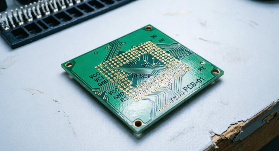
A PCB board prototype is an early production version of a printed circuit board used to verify circuit design, layout, materials, manufacturability, and assembly performance before mass production. For engineers and buyers, a well-planned prototype reduces design risk, prevents costly redesigns, and helps confirm whether a board can meet electrical, mechanical, thermal, and compliance requirements.
In practical electronics development, PCB prototyping is not just a sample-making step. It is the point where schematic assumptions, stack-up choices, component placement, signal integrity, solderability, and manufacturing tolerances are tested together. A good prototype process helps teams move from concept to production with fewer delays and fewer hidden quality problems.
What Is a PCB Board Prototype?
A PCB board prototype is a small-batch or sample PCB built to test whether a design can function correctly and be manufactured reliably. It may be a simple two-layer board for a consumer device, a high-density interconnect board for compact electronics, or a multilayer board for industrial, medical, automotive, communication, or AI hardware.
The main purpose is to validate the design before committing to tooling, volume purchasing, SMT assembly, functional testing, and full-scale production. Depending on the project stage, a prototype may focus on electrical verification, mechanical fit, firmware debugging, thermal behavior, connector alignment, or assembly process validation.
For many engineering teams, the first prototype is not expected to be perfect. Its value comes from exposing practical issues early, such as incorrect footprints, poor impedance planning, insufficient clearances, missing test points, overheating zones, or component sourcing risks.
Why PCB Board Prototypes Matter Before Production
PCB board prototypes matter because they help prevent expensive mistakes before mass production starts. A small design error that costs little to fix during prototyping can become a major quality, delivery, or warranty problem after thousands of boards are built.
In real manufacturing, many problems cannot be fully detected from a schematic alone. Trace width, copper thickness, via structure, solder mask clearance, panelization, warpage control, impedance matching, and component placement all affect the final performance of a PCB assembly. Prototype manufacturing gives engineers a physical board to test under real operating conditions.
For buyers, prototyping also confirms whether a PCB supplier can communicate clearly, review engineering files, identify manufacturability risks, and deliver consistent quality. This is especially important for OEM and ODM projects where the same design may later move into repeated batch production.
How the PCB Board Prototype Process Works
The PCB board prototype process usually starts with design files and ends with tested bare boards or assembled PCBA samples. The most common input files include Gerber files, drill files, PCB stack-up notes, BOM, pick-and-place files, assembly drawings, and special process requirements.
A typical prototype workflow includes design file review, engineering questions, material confirmation, CAM checking, panel preparation, inner layer imaging, lamination, drilling, plating, solder mask, surface finish, legend printing, routing, electrical testing, inspection, packing, and shipping. If assembly is required, SMT programming, solder paste printing, component placement, reflow soldering, AOI, manual inspection, and functional testing may also be included.
The most important step is the engineering review before production. Many prototype failures are caused not by manufacturing defects, but by design files that lack clear specifications. Board thickness, copper weight, impedance, surface finish, controlled depth milling, via filling, solder mask color, and tolerance requirements should be confirmed before fabrication begins.
Main Types of PCB Board Prototypes
PCB board prototypes can be classified by structure, layer count, application, material, and assembly complexity. Choosing the correct type depends on the electrical performance, mechanical space, heat dissipation, flexibility, and reliability requirements of the project.
| Prototype Type | Typical Application | Relative Cost | Key Limitation |
|---|---|---|---|
| Single-sided PCB prototype | Simple controls, LED boards, low-cost electronics | Low | Limited routing space and lower circuit density |
| Double-sided PCB prototype | Consumer electronics, sensors, power control boards | Low to medium | May not support complex high-speed routing |
| Multilayer PCB prototype | Industrial control, communication devices, servers | Medium to high | Requires accurate stack-up and impedance control |
| HDI PCB prototype | Wearables, compact modules, advanced consumer devices | High | Higher process complexity and tighter design rules |
| Flexible PCB prototype | Wearables, cameras, medical probes, foldable electronics | Medium to high | Requires careful bend radius and stiffener design |
| Rigid-flex PCB prototype | Automotive modules, aerospace electronics, compact devices | High | Complex stack-up and higher DFM requirements |
| Metal core PCB prototype | LED lighting, power electronics, thermal modules | Medium | Limited multilayer routing compared with FR-4 boards |
Common Materials Used in PCB Board Prototypes
The material choice affects electrical performance, thermal stability, cost, mechanical strength, and long-term reliability. FR-4 is the most common material for standard PCB board prototypes, but high-frequency, high-speed, flexible, and high-power applications often need specialized materials.
FR-4 is widely used for consumer electronics, industrial control boards, power supplies, and general digital circuits. Polyimide is commonly used for flexible PCBs because it supports bending and compact installation. Rogers and other high-frequency laminates are used in RF, radar, antenna, communication, and low-loss signal applications. Aluminum or copper substrates are often selected for LED lighting, power modules, and heat-sensitive circuits.
Material selection should not be based on price alone. If a board involves high-speed signals, controlled impedance, wide temperature exposure, high current, or repeated bending, the wrong laminate can cause signal loss, delamination, copper cracking, or thermal failure.
Key Design Factors for a Reliable PCB Board Prototype
A reliable PCB board prototype starts with clear design rules and complete engineering files. Even a strong manufacturer cannot compensate for missing footprints, unsafe spacing, unclear stack-up requirements, or incorrect assembly data.
Engineers should confirm trace width, spacing, via size, annular ring, copper balance, solder mask expansion, component-to-edge distance, impedance requirements, high-current paths, creepage distance, and thermal relief design. For assembly prototypes, footprint accuracy is especially important. A wrong pad size or polarity mark can delay testing even when the bare PCB is well made.
High-speed designs need additional care. Differential pairs, return paths, reference planes, via stubs, connector transitions, and layer stack-up should be planned early. Power electronics require attention to copper thickness, current capacity, heat spreading, isolation, and safety spacing. Flexible circuits require bend direction, bend radius, dynamic or static bending conditions, and stiffener placement to be clearly defined.
PCB Prototype Manufacturing Capabilities to Confirm
Before placing a PCB board prototype order, buyers should confirm whether the manufacturer can support the required layer count, copper thickness, minimum trace and spacing, via process, surface finish, material, impedance control, and testing method.
| Capability Item | Why It Matters | What to Confirm Before Ordering |
|---|---|---|
| Layer count | Determines routing density and stack-up complexity | Confirm standard and advanced multilayer capability |
| Copper thickness | Affects current capacity and thermal performance | Specify finished copper weight clearly |
| Minimum trace and spacing | Controls manufacturability and yield | Check whether the design matches factory rules |
| Via structure | Impacts routing, reliability, and cost | Confirm through via, blind via, buried via, or filled via needs |
| Surface finish | Affects solderability, shelf life, and fine-pitch assembly | Choose HASL, lead-free HASL, ENIG, OSP, immersion silver, or other finish |
| Impedance control | Critical for high-speed and RF circuits | Provide target impedance and stack-up requirements |
| Electrical test | Detects open and short circuits | Confirm 100% E-test for prototype and production lots |
Quality Standards and Testing for PCB Board Prototypes
Quality control for PCB board prototypes should follow recognized industry requirements and practical inspection methods. Common references include IPC standards for printed board workmanship, UL safety recognition where applicable, RoHS compliance for restricted substances, and project-specific customer specifications.
For bare PCB prototypes, standard checks may include CAM review, material verification, solder mask inspection, hole size measurement, copper thickness control, surface finish inspection, dimensional measurement, impedance testing when required, and 100% electrical testing. For PCBA prototypes, additional checks may include solder paste inspection, automated optical inspection, X-ray inspection for hidden solder joints, first article inspection, and functional testing.
Medical, automotive, aerospace, and industrial projects often need stricter documentation and process control. Certifications such as ISO 9001, ISO 13485, IATF 16949, UL recognition, and RoHS compliance can support supplier qualification, but buyers should still verify whether the selected process, material, and inspection plan match the actual project risk.
Common PCB Board Prototype Failures and How to Prevent Them
Many PCB board prototype failures come from design-for-manufacturing gaps rather than isolated factory defects. The best prevention is early engineering review before fabrication and assembly.
| Failure Issue | Common Cause | Prevention Method |
|---|---|---|
| Open circuit | Broken trace, over-etching, insufficient annular ring | Use proper trace width, review drill-to-pad tolerance, run E-test |
| Short circuit | Insufficient spacing, solder bridge, copper residue | Follow spacing rules, check solder mask clearance, inspect assembly |
| Poor solderability | Wrong surface finish, oxidation, long storage | Select suitable finish and control packing and shelf life |
| Signal instability | Poor impedance control, weak return path, bad stack-up | Define impedance, reference planes, and differential pair rules |
| Board warpage | Unbalanced copper, thin board, high reflow stress | Balance copper distribution and review panel design |
| Overheating | Insufficient copper area, poor thermal vias, wrong substrate | Improve copper pours, add thermal vias, consider metal core PCB |
| Component misalignment | Incorrect footprint, poor placement file, wrong polarity marking | Review BOM, centroid file, assembly drawing, and first article sample |
A practical prototype review should look beyond whether the board can be fabricated. It should ask whether the board can be assembled, tested, repaired, scaled, and repeated with stable yield. That is where experienced engineering support becomes valuable.
How to Choose the Right PCB Board Prototype for Your Project
The right PCB board prototype depends on the product function, signal speed, available space, operating environment, testing goals, and future production volume. A simple sensor board may only need a standard FR-4 double-sided PCB, while a compact wearable, automotive control module, or AI accelerator board may need HDI, rigid-flex, high-speed materials, or heavy copper.
If the product is still in early concept testing, a lower-cost prototype may be enough to verify basic functionality. If the design is close to mass production, the prototype should use the same materials, stack-up, surface finish, copper thickness, and assembly process planned for production. This avoids false confidence from a prototype that works but cannot be repeated at scale.
Buyers should also consider component availability. A PCB prototype can be delayed if one IC, connector, sensor, or power device has long lead time or limited supply. BOM optimization and approved alternative components are useful during prototype planning, especially for OEM and ODM projects.
Industry Applications of PCB Board Prototypes
PCB board prototypes are used across nearly every electronics sector because each industry has different reliability, cost, and compliance expectations. A prototype for a consumer product may focus on compact size and cost, while a prototype for automotive, medical, aerospace, or industrial use may focus on safety, traceability, and long-term stability.
In consumer electronics, prototypes are common for smart TVs, wearables, earbuds, cameras, smart home devices, and appliance control boards. These projects often use HDI, FPC, rigid-flex, or standard single and double-sided PCBs to meet thin, light, and high-density design goals.
In automotive electronics, prototypes may support BMS, VCU, MCU, OBC, ADAS sensors, radar, cameras, cockpit displays, lighting controls, and seat control modules. These boards often require high reliability, wide temperature tolerance, vibration resistance, thermal management, and automotive-grade process discipline.
In communication equipment, PCB prototypes are used for 5G and 6G base stations, optical modules, routers, switches, RF front ends, and server backplanes. These projects often require low-loss materials, controlled impedance, high multilayer counts, and precise signal integrity management.
In industrial control and automation, prototypes are used for PLCs, servo drives, inverters, robotics, machine vision, sensors, CNC machines, gateways, and instruments. Stability, EMC performance, long service life, and thermal reliability are often more important than the lowest unit price.
PCB Board Prototype Cost Factors
The cost of a PCB board prototype is affected by board size, layer count, material, copper thickness, surface finish, hole density, tolerance requirements, impedance control, delivery time, assembly complexity, and testing needs.
A standard two-layer FR-4 prototype is usually much less expensive than a multilayer HDI, rigid-flex, or high-frequency PCB prototype. Costs also increase when a design requires blind vias, buried vias, via filling, tight impedance tolerance, heavy copper, special laminate, small trace spacing, controlled depth milling, or advanced inspection.
For assembled prototypes, component sourcing can become a major cost driver. Low-volume component purchasing often has higher unit cost than mass production purchasing. Engineering teams can reduce cost by approving alternative components, avoiding unnecessary process complexity, and using production-friendly footprints from the beginning.
How to Select a PCB Prototype Manufacturer
A reliable PCB prototype manufacturer should provide more than quick fabrication. The supplier should review files carefully, identify design risks, communicate engineering questions clearly, support custom requirements, and maintain repeatable quality from prototype to mass production.
When comparing suppliers, buyers should check manufacturing capability, certification background, engineering response time, material options, assembly support, testing methods, traceability, packaging quality, and experience with similar applications. For cross-border sourcing, clear communication and complete file confirmation are especially important.
As a China-based source factory and global PCB/PCBA manufacturer, Thindry focuses on PCB fabrication, component sourcing, and PCB assembly support for prototype and production projects. With experience in consumer electronics, automotive electronics, communication equipment, industrial control, medical electronics, server hardware, LED lighting, and power electronics, our engineering team helps customers review manufacturability risks before production starts.
Checklist Before Ordering a PCB Board Prototype
Before ordering a PCB board prototype, prepare complete and consistent project files. Missing or conflicting information is one of the most common causes of prototype delay.
- Gerber files and drill files
- PCB stack-up and board thickness requirements
- Material grade and copper thickness
- Surface finish requirement
- Solder mask color and legend color
- Controlled impedance requirements, if any
- Special tolerance or mechanical requirements
- BOM with manufacturer part numbers
- Pick-and-place file for assembly
- Assembly drawing and polarity notes
- Testing requirements and acceptance criteria
- Expected prototype quantity and future production plan
If the prototype is intended for later mass production, it is better to discuss production volume, target cost, testing plan, and supply chain requirements during the prototype stage. This helps avoid redesign when the product moves from sample approval to batch manufacturing.
FAQ About PCB Board Prototype Projects
What is the difference between a PCB prototype and a production PCB?
A PCB prototype is built in small quantities to verify design, materials, dimensions, and assembly before mass production. A production PCB is manufactured in larger batches with stable process control, optimized cost, and repeatable quality. If a design is close to release, the prototype should use production-intent materials and processes.
How many PCB board prototypes should I order for testing?
The right quantity depends on your testing plan. Early design checks may need only a few bare boards, while firmware, assembly, thermal, reliability, and customer validation may require more samples. It is wise to include extra units for destructive testing, rework, and backup during debugging.
What files are required for a PCB board prototype order?
For bare PCB fabrication, Gerber files, drill files, board thickness, copper weight, material, surface finish, and special requirements are usually needed. For assembly, you should also provide BOM, pick-and-place files, assembly drawings, polarity notes, and test instructions.
Can a PCB prototype be used directly for mass production?
Sometimes yes, but only if the prototype was built with production-intent materials, stack-up, tolerances, and assembly processes. If the prototype used simplified rules or substitute materials, it should be reviewed again before mass production to avoid yield, reliability, or cost problems.
What surface finish is best for a PCB board prototype?
ENIG is often selected for fine-pitch components, good solderability, and longer shelf life. HASL or lead-free HASL may suit many general boards, while OSP can be cost-effective for certain applications. The best choice depends on assembly requirements, component pitch, storage time, and compliance needs.
Why does my PCB prototype fail even when the schematic is correct?
A correct schematic does not guarantee a working PCB. Layout issues, poor grounding, incorrect footprints, impedance mismatch, insufficient spacing, thermal problems, soldering defects, or missing test points can cause failure. This is why design-for-manufacturing and design-for-assembly reviews are important.
How can I reduce the cost of PCB board prototype manufacturing?
Use standard materials where possible, avoid unnecessary tight tolerances, reduce special via structures, choose practical surface finishes, and confirm component availability early. Cost should be optimized without weakening reliability, especially for power, automotive, medical, or industrial applications.
Is a two-layer PCB prototype enough for my project?
A two-layer PCB may be enough for simple circuits, low-speed signals, and basic control boards. Multilayer boards are usually better for high-density layouts, high-speed signals, stable power distribution, EMC control, and compact products. The final choice should match circuit complexity and performance risk.
What is controlled impedance in PCB prototypes?
Controlled impedance means the PCB trace geometry and stack-up are designed to maintain a target impedance for high-speed or RF signals. It is important for USB, Ethernet, DDR, RF, radar, and communication circuits. The manufacturer needs stack-up details and impedance targets before fabrication.
Can PCB prototype manufacturers also assemble components?
Yes, many PCB manufacturers offer PCB assembly prototype services, including SMT, through-hole assembly, mixed assembly, component sourcing, AOI, X-ray inspection, and functional testing. Using one supplier for PCB and PCBA can reduce communication gaps and speed up prototype validation.
What causes delays in PCB board prototype projects?
Common delays include incomplete Gerber files, missing stack-up information, unclear impedance requirements, unavailable components, incorrect BOM data, unconfirmed substitutions, and design rule conflicts. Fast delivery depends on complete files and quick responses to engineering questions.
How do I know if a PCB prototype supplier is reliable?
Check whether the supplier asks detailed engineering questions, provides clear capability limits, supports quality inspection, follows recognized standards, and has experience in your application field. A reliable supplier should help identify risks before production rather than simply accept files without review.
Should I test a bare PCB before assembly?
Yes, bare PCB electrical testing helps detect open and short circuits before components are mounted. For complex or expensive assemblies, bare board testing reduces the risk of wasting components and assembly time on defective boards. It is especially important for multilayer and high-density designs.
Final Thoughts on PCB Board Prototype Selection
A successful PCB board prototype is not only about fast delivery. It depends on correct material selection, complete design files, practical manufacturing rules, reliable testing, and clear communication between engineering, purchasing, and production teams. The best prototype strategy is to validate function while preparing the design for stable mass production.
If your project involves high-speed signals, compact layouts, thermal stress, automotive reliability, medical compliance, or industrial operating environments, involve your PCB manufacturer early. Early review can prevent footprint errors, stack-up problems, soldering defects, sourcing delays, and repeat redesign cycles.
If you’re sourcing reliable PCB/PCBA manufacturing — OEM, ODM, prototyping, mass production, or custom engineering solutions — reach out to our engineering team for technical support and a quote at sales@pcbtry.com.

0 Comments