
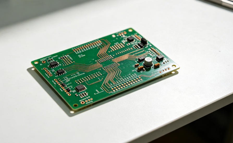
A PCB board is the bare board that makes an electronic circuit buildable, repeatable, and manufacturable.
Instead of wiring every connection by hand, the PCB prints those connections as copper paths on an insulating laminate. Components sit on pads. Copper traces connect pins. Vias move signals between layers. Solder mask protects the copper. Silkscreen helps people place, inspect, and service the board.
If you are searching for what is a pcb board, here is the practical answer: if a product has electronics inside, the PCB is usually where the real circuit lives.
It does more than hold parts. It routes signals, moves power, gives current a return path, supports components, controls heat, and keeps every unit built the same way.
That last point matters.
A hand-wired prototype may work once on a bench. A PCB lets the same circuit be built again and again with controlled geometry. That is the difference between a working idea and a product that can be manufactured.
The schematic tells you what should connect. The PCB layout decides how those connections behave in the real world.
A bad layout can ruin a good schematic. Engineers learn that quickly.
PCB Board vs Circuit Board vs PCBA
These terms get mixed up all the time, especially during quoting.
A PCB board usually means the bare printed circuit board. It has copper layers, drilled holes, plated vias, solder mask, silkscreen, and surface finish. No components are assembled yet.
A circuit board is a more general term. In daily use, many people use it to mean the same thing as a PCB.
A PCBA means printed circuit board assembly. That is the PCB after components have been mounted and soldered. Once resistors, capacitors, ICs, connectors, relays, LEDs, modules, or transformers are installed, the bare PCB becomes a PCBA.
The pcb board vs pcba difference matters because the job scope changes completely.
A PCB quote usually covers bare board fabrication only.
A PCBA quote may include PCB fabrication, component sourcing, SMT assembly, through-hole assembly, inspection, programming, functional testing, and packaging.
One easy way to lose two days is to send Gerbers and a BOM without saying whether you need bare boards or full assembly. The supplier has to stop and ask. The quote waits. The build waits.
Be clear at the beginning:
- Do you need PCB only?
- Do you need full PCBA?
- Do you need components sourced?
- Do you need testing?
- Do you need conformal coating, programming, or box build?
That small clarification saves real time.
Basic Structure of a Printed Circuit Board
The basic structure of a printed circuit board is simple on the surface, but every layer has a job.
Most PCB boards include these parts:
Laminate or Core Material
The core or laminate gives the board mechanical strength and electrical insulation. FR-4 is the standard choice for many commercial and industrial products. It is strong, cost-effective, and widely available.
Some applications need other materials. High-frequency circuits may need low-loss laminates. High-temperature products may need materials with better thermal stability. LED and power boards may use aluminum or metal-core structures to move heat away from components.
Copper Layers
Copper forms the actual circuit paths. Copper thickness is often specified in ounces, such as 1 oz or 2 oz. Higher copper can carry more current, but it also affects trace width, spacing, etching control, weight, and cost.
More copper is not always better. It helps with current and heat, but it can make fine features harder to manufacture. For high-current boards, copper weight should be reviewed together with trace width, temperature rise, board thickness, and thermal path.
Solder Mask
Solder mask is the colored coating over the copper. Green is common, but blue, black, red, white, and other colors are also used.
Its real job is not decoration. It protects copper and helps prevent solder bridges during assembly. For fine-pitch components, solder mask registration and opening size matter more than mask color.
Silkscreen
Silkscreen adds markings. Reference designators, polarity marks, pin 1 indicators, warnings, logos, and assembly notes all go here.
Bad markings slow down inspection. Wrong markings can cause assembly mistakes. A reversed diode symbol or missing pin 1 mark can waste more time than people expect.
Surface Finish
Surface finish protects exposed copper pads and makes soldering possible. Common choices include HASL, lead-free HASL, ENIG, OSP, immersion silver, and immersion tin.
The right finish depends on component type, shelf life, flatness requirements, cost, and assembly process. For example, ENIG is often preferred for fine-pitch parts, BGA packages, and flatter pad requirements.
Vias
Vias connect layers. They look small, but they are not minor details. Via size, plating, aspect ratio, and placement affect routing density, current capacity, impedance, yield, and reliability.
A PCB is built from boring details. Those boring details decide whether the board is easy to manufacture or painful to build.
What Is a PCB Board and How Does It Work?
The search phrase what is a pcb board and how does it work usually leads to a basic answer: a PCB connects electronic components.
That answer is true, but incomplete.
At board level, the PCB is doing several jobs at the same time.
- It carries signals between components.
- It distributes power.
- It gives return current a controlled path.
- It supports mechanical loads from connectors, switches, relays, and heavy components.
- It manages heat from power devices, LEDs, regulators, and high-current traces.
- It affects noise, EMI, and signal quality.
On a slow board, you can sometimes get away with ugly routing. Not always, but sometimes.
Once fast edges, switching regulators, high current, RF, or sensitive analog signals show up, copper shape starts to matter.
A switching power supply may use the right IC and still fail EMC because the hot loop is too large.
A microcontroller board may run on the bench and reset in the field because the ground path is weak.
A high-current board may pass a quick test but overheat inside a sealed enclosure.
A connector may pass electrical testing but crack solder joints because the board has no mechanical support.
This is why PCB layout is not paperwork. It is part of the circuit.
The schematic shows intent. The board layout decides whether that intent survives manufacturing, assembly, testing, shipping, and real use.
Common PCB Board Types and Where They Fit
Not every PCB needs the same construction. The right choice depends on the job the board has to do.
Single-Sided PCB
A single-sided PCB has copper on one side only. It is low cost and simple. It works for basic circuits, LED boards, simple power boards, and low-density products.
Double-Sided PCB
A double-sided PCB has copper on both sides. It gives more routing flexibility and is common in many control boards, power modules, and consumer devices.
Multilayer PCB
A multilayer PCB uses internal copper layers. Four-layer and six-layer boards are common when signal integrity, power integrity, dense routing, or EMI control matters.
A four-layer board with solid power and ground planes often performs better than a crowded two-layer board.
Aluminum PCB
An aluminum PCB uses a metal base to move heat away from components. It is common in LED lighting and some power applications.
Flexible PCB
A flexible PCB can bend. It is used where space is tight or movement is required, such as displays, cameras, wearable devices, sensors, and compact electronic assemblies.
Rigid-Flex PCB
A rigid-flex PCB combines rigid sections and flexible sections. It costs more, but it can reduce connectors, cable failures, and assembly complexity.
High-Frequency PCB
High-frequency PCB materials are used for RF, microwave, antenna, and controlled-loss applications. FR-4 is not always good enough when frequency and loss become critical.
Start with product risk, not the cheapest board option.
A low-cost board is fine if it meets the electrical, thermal, and mechanical needs. But the wrong stackup or material usually shows its cost later as rework, unstable performance, late delivery, or field returns.
Design Details That Decide Whether a PCB Can Be Built
A PCB design is not ready for production just because the layout is complete.
Before release, check the details that factories actually care about:
- Trace width
- Trace spacing
- Drill size
- Annular ring
- Copper-to-edge clearance
- Solder mask opening
- Board thickness
- Copper weight
- Controlled impedance
- Surface finish
- Panelization
- Slot and cutout dimensions
- Via type
- Component clearance
These items look small in CAD. In production, they decide price, yield, and lead time.
Do not design 3 mil traces unless you actually need them and your supplier can hold them in production. Fine lines look harmless on screen. They reduce process margin on the factory floor.
Very small holes can increase cost. High aspect ratio vias can reduce plating reliability. Weak annular rings can create breakout risk. Tight copper-to-edge spacing can cause quality issues after routing.
Footprints are another common source of trouble.
Bad footprints are one of the fastest ways to turn a clean PCB into an assembly problem. Pads that are too large may cause tombstoning. Pads that are too small may create weak solder joints. Wrong polarity marks can scrap an entire batch.
Mechanical details matter too. Connectors, switches, transformers, relays, and heavy components need enough support. If a board will be plugged, pulled, vibrated, or mounted into an enclosure, layout should consider mechanical stress from the beginning.
Manufacturing is not separate from design. The factory only builds what the files tell it to build.
Common Mistakes New PCB Buyers Make
Many PCB problems start before the order is placed.
Here are mistakes that slow down quoting and production:
- Sending Gerber files without a stackup requirement
- Not specifying copper weight
- Forgetting board thickness
- Leaving controlled impedance unclear
- Using incomplete BOM data for PCBA
- Providing no pick-and-place file for assembly
- Not confirming component polarity
- Choosing a surface finish without considering assembly
- Ignoring panelization for SMT production
- Assuming the cheapest quote includes testing
For prototypes, these mistakes may only cost a few days.
For production, they can cost much more: delayed launch, extra freight, scrapped boards, manual rework, unstable yield, and difficult quality disputes.
A strong PCB supplier should not only take files and quote a price. The supplier should help catch practical issues before the build starts.
PCB Cost Drivers Buyers Should Understand
PCB price is not decided by board size alone.
The following factors can change cost quickly:
- Layer count
- Board size and panel utilization
- Material type
- Copper thickness
- Minimum trace width and spacing
- Smallest drill size
- Surface finish
- Controlled impedance requirements
- Blind, buried, or filled vias
- Special processes such as via-in-pad or edge plating
- Quantity
- Lead time
- Testing requirements
A cheaper quote may be completely reasonable. It may also be missing something.
Before comparing prices, make sure every supplier is quoting the same technical requirement. A 2-layer FR-4 PCB with HASL is not the same job as a 4-layer impedance-controlled PCB with ENIG and tight drilling tolerances.
For PCBA, the cost picture changes again. Component sourcing, SMT setup, stencil, fixture, inspection, programming, functional testing, and packaging can all affect the final quote.
If the quote looks too low, check the scope before celebrating.
PCB Quality Checks Before Production
Before a PCB goes into production, the supplier should check more than file readability.
A proper review may include:
- Gerber file check
- Drill file check
- Layer alignment review
- Minimum trace and spacing review
- Annular ring review
- Solder mask clearance check
- Silkscreen-to-pad clearance check
- Board outline and slot review
- Stackup confirmation
- Impedance requirement confirmation
- Panelization review
- BOM and footprint consistency check for PCBA
For assembly projects, the review should go further.
The supplier should check component availability, package matching, polarity, placement orientation, soldering method, thermal relief, and possible assembly interference.
These checks do not make the design perfect. But they reduce obvious production risk.
That is often the difference between a smooth build and a week of back-and-forth emails.
When You Should Request a DFM Review
A DFM review is useful when the cost of a mistake is higher than the cost of checking early.
You should request a DFM review if:
- This is your first build with a new design
- The board has fine-pitch components
- The PCB uses BGA, QFN, or dense SMT parts
- The board carries high current
- The product has thermal concerns
- The board requires controlled impedance
- The layout uses blind vias, buried vias, or via-in-pad
- The design will move from prototype to production
- The product has reliability or compliance requirements
- You are not sure whether your Gerber, BOM, and assembly files are complete
A good DFM review does not just say “pass” or “fail.” It should tell you what may cause manufacturing difficulty, assembly risk, cost increase, or yield loss.
That feedback is valuable before fabrication. After fabrication, it becomes rework.
How Thindry Supports Custom PCB and PCBA Projects
Thindry supports custom PCB manufacturing and PCBA assembly for prototypes, small batches, and production projects.
Our team can help with bare PCB fabrication, component sourcing, SMT assembly, through-hole assembly, inspection, testing support, and production communication.
Every project is different. Some customers need a simple 2-layer PCB. Some need multilayer boards, controlled impedance, aluminum PCB, flexible PCB, or full turnkey PCBA. Some already have complete files. Others need a manufacturability check before ordering.
Thindry can support customized requirements based on your design files, application needs, quantity, lead time, and quality expectations.
We can also provide a free DFM report to help you identify potential production risks before the build starts.
If you are preparing a new PCB or PCBA project, you can send your Gerber files, BOM, pick-and-place file, drawings, or technical requirements to:
Email: sales@pcbtry.com
Our team will review your files and help you confirm the next step.
FAQ About PCB Boards
What is a PCB board in simple words?
A PCB board is a board that holds electronic components and connects them with copper traces. It replaces loose wiring with printed copper paths, making the circuit easier to build, inspect, and repeat.
Is a PCB the same as a circuit board?
In many conversations, yes. People often use PCB and circuit board to mean the same thing. Technically, PCB usually refers to a printed circuit board, while circuit board is a broader everyday term.
What is the difference between PCB and PCBA?
A PCB is the bare board without components. A PCBA is the assembled board with components soldered onto it. If you need a working electronic module, you usually need PCBA, not just PCB fabrication.
What materials are used in PCB boards?
Common PCB materials include FR-4 laminate, copper foil, solder mask, silkscreen ink, and surface finish materials such as HASL, ENIG, OSP, immersion silver, or immersion tin. Some boards use aluminum, flexible materials, or high-frequency laminates.
Why are some PCB boards more expensive than others?
Cost depends on layer count, board size, material, copper weight, trace width, spacing, drill size, surface finish, impedance control, special via structures, quantity, and lead time. For PCBA, component cost and assembly complexity also matter.
Do I need a DFM review before ordering PCB boards?
You should request a DFM review if the board is new, dense, high-current, high-speed, impedance-controlled, or moving toward production. A DFM review can catch manufacturability and assembly risks before money is spent on fabrication.
What files are needed for a PCB quote?
For bare PCB fabrication, Gerber files and drill files are usually required. A fabrication drawing is also helpful. For PCBA, you should also provide the BOM, pick-and-place file, assembly drawing, and any testing or programming requirements.
Can Thindry help with both PCB and PCBA?
Yes. Thindry can support custom PCB fabrication and PCBA assembly, including component sourcing, SMT assembly, through-hole assembly, inspection, and project review. You can contact sales@pcbtry.com for a quotation or free DFM review.
Final Thoughts
A PCB board is not just a green board with copper lines. It is where the circuit becomes a physical product.
The design choices behind that board affect noise, heat, current flow, soldering quality, mechanical strength, cost, lead time, and long-term reliability.
If you only need a definition, a PCB is a printed circuit board.
If you are building a real product, the better question is: can this PCB be manufactured, assembled, tested, and used reliably?
That question is where good engineering and good manufacturing support matter.
If you need custom PCB or PCBA support, Thindry can review your files and provide a free DFM report before production.
Send your project files or requirements to sales@pcbtry.com.


0 Comments