
What is PCB Testing and Why Does It Matter for Circuit Board Production
PCB testing refers to standardized inspection and validation workflows that verify printed circuit board structural integrity, electrical stability, and functional compliance with original design standards. Understanding what is PCB testing empowers hardware designers, production engineers, and supply chain specialists to locate hidden circuit defects, reduce product failure rates, and deliver stable, high-performance electronic hardware.
All custom PCB fabrication and finished PCBA assemblies require rigorous PCB testing before prototype delivery or large-scale mass production. Comprehensive testing effectively detects open circuits, short circuits, faulty solder joints, misaligned components, and poor electrical conductivity. Reliable PCB quality testing greatly reduces post-production malfunctions and costly electronic device recalls.
What Are the Main Types of Professional PCB Testing Methods
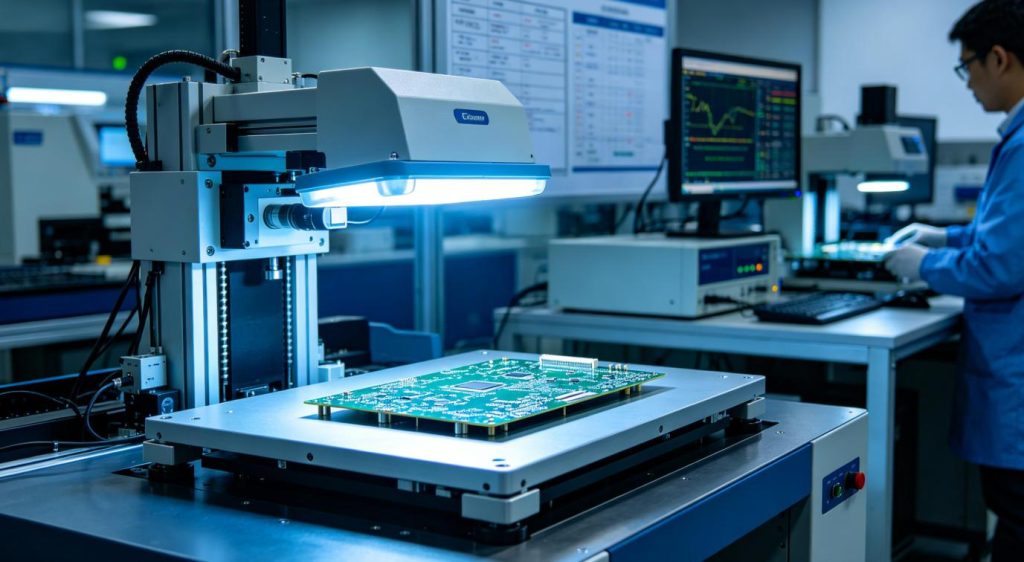
Common professional PCB testing methods are categorized into visual inspection, electrical verification, and functional performance testing. Each testing technique targets unique manufacturing and assembly defects at different production phases. Selecting the right PCB testing solution based on production volume and end-use industry delivers precise defect detection and efficient quality control.
| Testing Method | Core Function | Best Production Scenario | Detectable Defects |
|---|---|---|---|
| Automated Optical Inspection (AOI) | Visual surface scanning for component and solder issues | Mass production, post-soldering inspection | Missing components, offset placement, cold solder joints, surface scratches |
| X-Ray Inspection | Non-destructive internal structure detection | High-density multilayer PCB, BGA packaging boards | Hidden solder voids, internal short circuits, invisible assembly flaws |
| In-Circuit Testing (ICT) | Electrical parameter verification of individual components | High-volume standardized PCBA production | Wrong component values, circuit continuity faults, short/open circuits |
| Flying Probe Testing | Flexible electrical testing without fixed fixtures | Prototypes, low-volume custom PCB orders | Circuit connection errors, impedance mismatches, layout faults |
| Functional Circuit Testing (FCT) | Full operational simulation under real working conditions | Finished product quality confirmation | Overall functional failure, signal instability, power supply anomalies |
How Does PCB Testing Benefit Different Electronic Industry Applications
Industry-specific PCB testing protocols provide customized quality assurance for mainstream electronic sectors, solving unique environmental tolerance and performance stability risks. The four most demanding industries requiring strict PCB quality testing include consumer electronics, automotive electronics, industrial automation systems, and medical electronic equipment.
Consumer Electronics
Miniaturized PCBs used in smartwatches, wireless Bluetooth headsets, and portable power devices rely on strict PCB testing to eliminate short-circuit risks from dense compact wiring. Targeted testing ensures low power consumption and consistent signal stability for long-term daily consumer device operation.
Automotive Electronics
Vehicle control PCBs and automotive sensor PCBA assemblies undergo specialized PCB testing, including high-temperature resistance and anti-vibration performance verification. This rigorous testing prevents circuit failure during vehicle operation and meets strict automotive industry safety certification standards.
Industrial Control & Automation
PCB testing for industrial signal acquisition and control circuit boards prioritizes anti-interference performance and continuous operational stability. Standardized industrial PCB testing avoids signal distortion and unexpected equipment shutdowns in harsh electromagnetic industrial environments.
Medical Electronics
PCBs built for medical diagnostic and patient monitoring devices require stringent PCB testing to guarantee error-free operation. Professional testing eliminates circuit signal interference and data inaccuracies, fully complying with strict medical electronics safety and reliability specifications.
What PCB Testing Standards Must Be Followed for Qualified Circuit Boards
Unified PCB testing standards establish universal inspection benchmarks for all fabricated bare boards and fully assembled circuit boards. These industry standards ensure consistent quality between prototype samples and mass-produced units. All certified PCB and PCBA manufacturing projects adhere to these rules to meet global safety and performance criteria.
- IPC-A-600: Defines visual quality acceptance criteria for bare PCB boards, covering trace integrity, solder mask quality, and surface defects
- IPC-A-610: Specifies assembly quality standards for PCBA, governing solder joint quality and component installation accuracy
- Environmental Reliability Standards: Includes temperature cycling, humidity resistance, and vibration testing for industrial and automotive-grade PCBs
Strict implementation of these standards eliminates unqualified products and ensures every delivered board matches design performance expectations.
What Common PCB Testing Errors Affect Final Product Quality
Most post-production PCB quality failures originate from incompletePCB testing workflows and insufficient defect inspection coverage. Identifying these common testing mistakes helps design and manufacturing teams optimize quality control processes, raise product yield rates, and deliver more durable circuit board products.
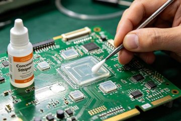
Incomplete visual inspection often misses tiny trace cracks and minor solder defects, which gradually expand during equipment operation. Skipping functional testing leads to undiscovered signal delay and power load faults under actual working conditions.
Using mismatched testing fixtures for custom PCBs causes inaccurate electrical parameter readings. Many low-volume prototype projects ignore reliability stress testing, resulting in poor environmental adaptability of finished boards.
How to Optimize PCB Testing Workflows for Higher Yield & Reliability
Optimizing PCB testing workflows is a proven method to cut manufacturing defects and boost operational efficiency for custom prototype PCBs and large-batch PCBA production. A layered, multi-stage PCB testing workflow delivers maximum detection accuracy and long-term product reliability for all circuit board projects.
Start with AOI visual inspection to eliminate surface assembly defects in the early production stage. Conduct flying probe or ICT electrical testing to verify circuit continuity and component parameter accuracy.
Finalize production quality control with FCT functional simulation and environmental reliability testing for high-end industrial, medical, and automotive PCBs. We support on-demand customization and can provide free DFM reports to improve PCB design testability upfront, effectively reducing PCB testing failures and production risks.
What Is the Difference Between Bare PCB Testing and PCBA Testing
Bare PCB testing and PCBA testing are two core quality control stages with distinct inspection goals, both critical for full-range circuit board quality assurance. Bare board testing verifies fabrication integrity, while PCBA testing validates assembly precision and complete functional performance of finished circuit boards.
| Testing Type | Testing Stage | Core Inspection Focus | Main Testing Methods |
|---|---|---|---|
| Bare PCB Testing | Post PCB fabrication, before component assembly | Trace integrity, hole conductivity, substrate quality, short/open circuits | Visual inspection, electrical continuity testing |
| PCBA Testing | Post component soldering and assembly | Component accuracy, solder quality, overall circuit function | AOI, X-Ray, ICT, Flying Probe, FCT |
FAQ: Frequently Asked Questions About PCB Testing
What is the main purpose of PCB testing?
The core objective of professional PCB testing is to detect hidden manufacturing and assembly defects, validate electrical functionality against design blueprints, and sustain stable long-term performance for electronic devices. Comprehensive PCB quality testing removes unqualified units and minimizes post-launch operational faults.
Is PCB testing necessary for prototype PCB orders?
Yes, detailed PCB testing is mandatory for all prototype PCB orders. Prototype PCB testing verifies design rationality, catches layout flaws and circuit faults at an early stage, and avoids costly repeated modifications during subsequent mass production.
Which PCB testing method is best for high-volume production?
Combined In-Circuit Testing (ICT) and AOI visual inspection is the most efficient PCB testing solution for high-volume production lines. This dual testing method offers fast detection speed, high precision, and stable batch inspection results ideal for standardized large-scale PCB manufacturing.
Can PCB testing detect hidden internal solder defects?
Basic visual inspection cannot detect internal hidden flaws, but professional X-Ray PCB testing accurately identifies hidden solder voids, BGA connection defects, and internal short circuits inside high-density multilayer PCBs.
How to improve the accuracy of custom PCB testing?
You can enhance custom PCB testing accuracy by optimizing design testability in advance, adopting customized testing methods based on board complexity, and combining multiple testing processes to cover all potential circuit and assembly defects.
If you have any demands for high-quality PCB and PCBA customization, prototype proofing, and mass production services, partner with Thindry for reliable full-cycle manufacturing and professional PCB testing support. We support on-demand customization and can provide free DFM reports for all PCB projects to boost design testability and production yield. Send your detailed project requirements to our email: sales@pcbtry.com.
0 Comments